PCB Chip Mounting: Techniques, Processes, and Advancements
Introduction
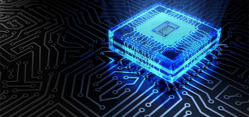
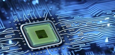
Printed Circuit Board (PCB) chip mounting is a critical process in electronics manufacturing that involves attaching semiconductor chips or integrated circuits (ICs) onto a PCB. This process ensures electrical connectivity, mechanical stability, and thermal management, enabling the functionality of electronic devices. With the rapid advancement of technology, PCB chip mounting techniques have evolved to meet the demands of miniaturization, high-speed performance, and reliability.
This article explores the key methods of PCB chip mounting, including surface-mount technology (SMT) and through-hole technology (THT), the mounting process, challenges, and emerging trends in the industry.
1. PCB Chip Mounting Methods
1.1 Surface-Mount Technology (SMT)
Surface-mount technology (SMT) is the most widely used method for mounting chips on PCBs. Unlike traditional through-hole mounting, SMT components are placed directly onto the surface of the PCB, allowing for higher component density and better performance in high-frequency applications.
Advantages of SMT:
- Smaller component size – Enables miniaturization of electronic devices.
- Higher circuit density – More components can be mounted per unit area.
- Better performance at high frequencies – Shorter lead lengths reduce parasitic inductance and capacitance.
- Automated assembly – Suitable for high-volume production.
Common SMT Components:
- Resistors, capacitors, and inductors (in tiny packages like 0201, 0402)
- Integrated circuits (QFN, BGA, CSP packages)
- Microcontrollers and memory chips
1.2 Through-Hole Technology (THT)
Through-hole technology (THT) involves inserting component leads into drilled holes on the PCB and soldering them on the opposite side. While less common in modern high-density designs, THT is still used for components requiring strong mechanical bonds or high power handling.
Advantages of THT:
- Strong mechanical connections – Ideal for high-stress environments.
- Easier manual assembly and repair – Suitable for prototyping and low-volume production.
- Better thermal and electrical performance for high-power components.
Common THT Components:
- Large capacitors and transformers
- Connectors and switches
- High-power semiconductors
1.3 Mixed Technology (SMT + THT)
Many PCBs use a combination of SMT and THT to leverage the benefits of both methods. For example, a motherboard may use SMT for most ICs while relying on THT for power connectors.
2. The PCB Chip Mounting Process
The chip mounting process varies depending on the technology used (SMT or THT), but generally follows these key steps:
2.1 SMT Assembly Process
- Solder Paste Application
- A stencil is used to apply solder paste onto the PCB pads.
- The paste consists of tiny solder balls mixed with flux.
- Component Placement
- A pick-and-place machine accurately positions SMD components onto the solder paste.
- Vision systems ensure proper alignment.
- Reflow Soldering
- The PCB passes through a reflow oven, melting the solder paste and forming permanent connections.
- Inspection and Testing
- Automated Optical Inspection (AOI) checks for defects like misalignment or solder bridges.
- Functional testing verifies electrical performance.
2.2 THT Assembly Process
- Component Insertion
- Components are manually or automatically inserted into pre-drilled holes.
- Wave Soldering
- The PCB passes over a wave of molten solder, which bonds the leads to the pads.
- Cleaning and Inspection
- Excess flux is removed, and the board is inspected for defects.
3. Challenges in PCB Chip Mounting
Despite advancements, several challenges persist in PCB chip mounting:
3.1 Miniaturization and High-Density Interconnects
- As components shrink (e.g., 01005 resistors), precise placement becomes more difficult.
- Fine-pitch BGAs and QFNs require advanced soldering techniques.
3.2 Thermal Management
- High-power chips generate heat, requiring efficient thermal vias and heat sinks.
- Warping due to thermal expansion can affect solder joint reliability.
3.3 Soldering Defects
- Solder bridges – Unintended connections between pins.
- Tombstoning – One end of a component lifts during reflow.
- Cold joints – Poor solder connections due to insufficient heat.
3.4 Component Compatibility
- Mixing SMT and THT components requires careful process planning.
- Different thermal profiles may affect solder joint integrity.
4. Emerging Trends in PCB Chip Mounting
4.1 Advanced Packaging Technologies
- System-in-Package (SiP) – Multiple chips integrated into a single package.
- 3D IC Stacking – Chips are vertically stacked for higher performance.
4.2 Automation and AI in Assembly
- AI-driven inspection systems improve defect detection.
- Robotics enhance precision in pick-and-place operations.
4.3 Flexible and Stretchable Electronics
- Flexible PCBs require new mounting techniques for bendable circuits.
4.4 Environmentally Friendly Manufacturing
- Lead-free soldering and halogen-free PCBs comply with RoHS regulations.
5. Conclusion
PCB chip mounting is a fundamental aspect of modern electronics manufacturing, with SMT dominating high-density applications and THT remaining relevant for high-power and mechanical robustness. As technology advances, new challenges and solutions emerge, driving innovation in packaging, automation, and material science.
The future of PCB chip mounting lies in smarter manufacturing processes, advanced packaging, and sustainable practices, ensuring that electronic devices continue to become smaller, faster, and more reliable.