Embedded Component PCB: Revolutionizing Modern Electronics Design
Introduction
The rapid advancement of electronics demands higher performance, miniaturization, and improved reliability in printed circuit board (PCB) design. One of the most innovative solutions addressing these challenges is the Embedded Component PCB (ECPCB), where passive and active components are integrated directly within the PCB substrate rather than being mounted on the surface. This technology offers significant advantages in terms of space savings, signal integrity, and thermal management, making it a key enabler for next-generation electronic devices.
This article explores the concept of Embedded Component PCBs, their benefits, manufacturing processes, applications, and future trends.
1. What is an Embedded Component PCB?
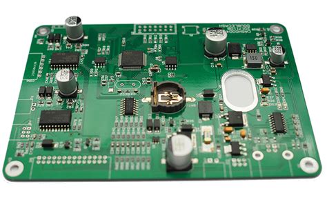
An Embedded Component PCB (ECPCB) is a multilayer PCB that incorporates electronic components (such as resistors, capacitors, inductors, and even ICs) inside the substrate layers rather than placing them on the surface. This integration is achieved using specialized fabrication techniques, allowing for a more compact and efficient design.
Types of Embedded Components
- Embedded Passive Components: Resistors, capacitors, and inductors embedded within the PCB layers.
- Embedded Active Components: Semiconductor devices (e.g., ICs, transistors) integrated into the PCB structure.
- Embedded Discrete Components: Individual components placed inside cavities within the PCB.

2. Advantages of Embedded Component PCBs
2.1 Miniaturization and Space Efficiency
By embedding components inside the PCB, designers can significantly reduce the board’s footprint. This is especially crucial for portable devices like smartphones, wearables, and IoT sensors, where space is at a premium.
2.2 Improved Signal Integrity
Shorter interconnects between embedded components reduce parasitic inductance and capacitance, leading to better high-frequency performance. This is vital for high-speed digital circuits and RF applications.
2.3 Enhanced Thermal Management
Embedding components distributes heat more evenly across the PCB, reducing hotspots and improving thermal dissipation. This enhances reliability, especially in power electronics and high-performance computing.
2.4 Increased Reliability and Durability
Since embedded components are protected within the PCB layers, they are less susceptible to mechanical stress, vibration, and environmental factors like moisture and dust.
2.5 Reduced Assembly Complexity
Fewer surface-mounted components simplify the assembly process, lowering manufacturing costs and improving yield rates.
3. Manufacturing Process of Embedded Component PCBs
The fabrication of ECPCBs involves several advanced techniques:
3.1 Laser Drilling and Cavity Formation
Precision laser drilling creates cavities within the PCB substrate where components are placed.
3.2 Component Embedding Techniques
- Resistor Embedding: Thin-film or thick-film resistors are printed directly onto inner layers.
- Capacitor Embedding: High-K dielectric materials are used to form planar capacitors between layers.
- Inductor Embedding: Spiral traces are designed within the PCB layers to create inductive elements.
- Active Component Embedding: Bare dies or packaged ICs are placed in cavities and interconnected using microvias.
3.3 Lamination and Layer Bonding
After component placement, additional dielectric and conductive layers are laminated under high pressure and temperature to encapsulate the embedded parts.
3.4 Via Formation and Interconnection
Microvias and through-holes are drilled and plated to establish electrical connections between embedded components and surface layers.
3.5 Surface Finishing and Testing
Final surface finishes (e.g., ENIG, HASL) are applied, followed by rigorous electrical and thermal testing to ensure performance and reliability.
4. Applications of Embedded Component PCBs
4.1 Consumer Electronics
- Smartphones & Tablets: Enables slimmer designs with better battery life.
- Wearables: Supports compact, lightweight designs for smartwatches and fitness trackers.
4.2 Automotive Electronics
- ADAS (Advanced Driver Assistance Systems): Improves signal integrity for radar and LiDAR systems.
- Electric Vehicles (EVs): Enhances power distribution and thermal management in battery control modules.
4.3 Aerospace and Defense
- Avionics: Reduces weight while maintaining high reliability in harsh environments.
- Military Communications: Ensures robust performance in high-frequency applications.
4.4 Medical Devices
- Implantable Electronics: Provides biocompatible, miniaturized PCBs for pacemakers and neurostimulators.
- Diagnostic Equipment: Enhances signal accuracy in MRI and ultrasound systems.
4.5 High-Performance Computing (HPC) & Data Centers
- Server Boards: Reduces latency and improves power efficiency in AI and cloud computing hardware.
5. Challenges and Limitations
Despite its advantages, Embedded Component PCB technology faces several challenges:
5.1 Higher Manufacturing Complexity
Specialized equipment and processes increase production costs compared to traditional PCBs.
5.2 Design Complexity
Accurate simulation and modeling are required to ensure proper electrical and thermal performance.
5.3 Rework and Repair Difficulties
Once components are embedded, repairing or replacing them is nearly impossible, requiring stringent quality control.
5.4 Limited Standardization
The lack of industry-wide standards for embedded components can hinder widespread adoption.
6. Future Trends in Embedded Component PCB
6.1 Advanced Materials
- Flexible and Stretchable Substrates: Enables bendable electronics for wearables and medical applications.
- High-Thermal-Conductivity Dielectrics: Improves heat dissipation in high-power designs.
6.2 3D Printed Embedded Electronics
Additive manufacturing techniques could revolutionize rapid prototyping and customization of ECPCBs.
6.3 AI-Driven Design Optimization
Machine learning algorithms will help optimize component placement and routing for better performance.
6.4 Heterogeneous Integration
Combining embedded components with system-in-package (SiP) and chiplets for next-gen computing.
6.5 Wider Industry Adoption
As costs decrease and standards emerge, ECPCBs will become mainstream in automotive, 5G, and IoT applications.
Conclusion
Embedded Component PCB technology represents a significant leap forward in electronics design, offering unparalleled miniaturization, performance, and reliability. While challenges remain in manufacturing complexity and standardization, ongoing advancements in materials, fabrication techniques, and design tools are paving the way for broader adoption.
As the demand for smaller, faster, and more efficient electronic devices grows, Embedded Component PCBs will play a crucial role in shaping the future of consumer electronics, automotive systems, medical devices, and beyond. Engineers and manufacturers must continue innovating to unlock the full potential of this transformative technology.