Advanced PCB Design & Manufacturing: Best Practices for Quality Output

Key Takeaways
Successful PCB design & manufacturing hinges on balancing technical precision with strategic planning. A core focus lies in material selection, where factors like thermal stability, dielectric properties, and cost efficiency dictate performance. For instance, high-frequency applications demand low-loss substrates like Rogers 4350B, while cost-sensitive projects may prioritize FR-4.
Integrating DFM (Design for Manufacturability) checks early minimizes rework, ensuring designs align with PCB assembly capabilities. Key DFM considerations include trace-width tolerances, solder mask clearances, and component placement spacing. Below is a comparison of common DFM pitfalls and solutions:
| DFM Challenge | Optimized Approach |
|---|---|
| Insufficient pad spacing | Adhere to PCBA vendor guidelines |
| Overly complex layer stack | Simplify with symmetric configurations |
| Inadequate thermal relief | Use spoke-based thermal connections |
Quality control processes, such as automated optical inspection (AOI) and X-ray testing, are critical for identifying defects in PCB assembly. Additionally, adopting automated workflows for tasks like panelization reduces human error and accelerates production. By harmonizing material selection, DFM compliance, and rigorous testing, manufacturers achieve reliable circuit boards that meet both performance benchmarks and cost targets.
Optimizing PCB Material Selection Strategies
Effective PCB assembly begins with strategic material selection, as substrate properties directly influence thermal performance, signal integrity, and long-term reliability. Key considerations include dielectric constant (Dk), loss tangent (Df), and coefficient of thermal expansion (CTE), which must align with operational demands such as high-frequency applications or extreme temperature environments. For instance, FR-4 remains a cost-effective choice for standard PCBA projects, while polyimide or Rogers substrates excel in high-speed or flexible designs.
Material compatibility with soldering processes and chemical exposure during manufacturing is equally critical. Laminates with low Z-axis expansion reduce via cracking risks during thermal cycling, while copper foil roughness impacts impedance control in high-frequency layouts. Engineers should prioritize materials certified under IPC-4101 standards to ensure consistency across PCB assembly batches.
Collaboration between design and PCBA teams enhances material optimization—for example, selecting halogen-free laminates for eco-compliance without compromising flame retardancy. Advanced simulation tools now predict material behavior under stress, enabling data-driven choices that balance performance, manufacturability, and cost. This proactive approach minimizes redesigns and aligns with downstream processes like automated optical inspection (AOI) and functional testing.
Implementing Effective DFM Guidelines
Adhering to Design for Manufacturability (DFM) principles ensures seamless transition from schematic concepts to functional PCB assembly outcomes. A critical first step involves analyzing component placement and trace routing to minimize signal interference and thermal stress during PCBA processes. Designers must prioritize standardized footprints and avoid overly dense layouts, which can complicate solder paste application and increase defect risks.
Integrating automated DFM validation tools early in the design phase helps identify issues like insufficient annular ring widths or mismatched pad sizes before prototyping. For instance, impedance-controlled routing demands precise material selection to align with manufacturing capabilities, reducing rework costs. Collaboration between design and PCB assembly teams is vital to balance performance requirements with production feasibility, such as optimizing panelization for higher yield.
Additionally, considering thermal management early—through proper via placement and copper balancing—prevents warping during reflow soldering. Clear documentation of layer stack-ups and finish specifications (e.g., ENIG or HASL) further streamlines communication with PCBA partners. By embedding DFM checks at every stage, engineers can mitigate delays, enhance reliability, and ensure compliance with industry standards like IPC-A-600. This proactive approach not only accelerates time-to-market but also fortifies the foundation for scalable, high-quality manufacturing workflows.
Streamlining PCB Manufacturing Workflows
Efficient PCB assembly processes rely on harmonizing design intent with production realities. By integrating digital twin simulations and automated design-for-manufacturing (DFM) analysis, engineers can preemptively address potential bottlenecks in PCBA workflows. Modern factories leverage intelligent process control systems to synchronize solder paste application, component placement, and reflow profiling—reducing human error while maintaining ISO-grade consistency.
Central to workflow optimization is the adoption of unified PCB assembly platforms that bridge CAD data with manufacturing execution systems (MES). These tools enable real-time tracking of thermal management parameters and signal integrity metrics during PCBA stages, ensuring compliance with IPC-6012 standards. Strategic implementation of modular fixturing and standardized panelization layouts further accelerates throughput without compromising precision.
Forward-thinking manufacturers are now embedding machine learning algorithms into PCB assembly lines to predict equipment maintenance needs and optimize material utilization. This data-driven approach, combined with lean inventory practices for high-frequency laminates and surface finish materials, reduces cycle times by up to 30% in complex PCBA projects. Crucially, maintaining open feedback loops between design teams and production floors ensures continuous refinement of manufacturing protocols—a critical factor in scaling high-mix, low-volume operations profitably.
Ensuring Circuit Board Reliability Standards
Achieving consistent reliability in PCB assembly requires adherence to rigorous design and manufacturing protocols. Critical factors include thermal management strategies, such as optimizing copper weight and via placement to dissipate heat effectively, and selecting materials with high glass transition temperatures (Tg) to withstand operational stress. For PCBA applications, ensuring proper solder joint integrity through precise reflow profiling and inspection techniques minimizes failure risks in high-vibration environments.
Tip: Implement automated optical inspection (AOI) during PCB assembly to detect micro-cracks or misalignments before final testing. This reduces rework costs and enhances long-term performance.
Environmental resilience is equally vital. Conformal coatings and encapsulation materials should be chosen based on the end-use environment—whether resisting humidity, chemical exposure, or extreme temperatures. Additionally, comprehensive design for reliability (DFR) practices, such as derating component loads and incorporating redundancy for critical circuits, strengthen PCBA durability.
Transitioning from design to production, manufacturers must validate reliability through accelerated life testing (ALT) and thermal cycling simulations. These tests identify weaknesses in PCB assembly processes, such as solder fatigue or layer delamination, enabling iterative improvements. Finally, maintaining traceability via serialized lot tracking ensures rapid root-cause analysis if field failures occur, closing the loop on quality assurance.
Advanced Quality Control Process Breakdown
Modern PCB assembly relies on a multi-layered quality control framework to mitigate defects and ensure compliance with industry standards. Automated Optical Inspection (AOI) systems form the first line of defense, scanning for surface-level issues like solder bridging or misaligned components. For internal integrity, X-ray inspection validates PCBA layer alignment, via connectivity, and hidden solder joint quality—critical for high-density designs. Electrical testing, including In-Circuit Testing (ICT) and Boundary Scan, verifies functional performance by simulating real-world operating conditions.
To address reliability, environmental stress screening (ESS) exposes boards to thermal cycling, vibration, and humidity, identifying weaknesses in material or PCB assembly processes. Advanced manufacturers also employ statistical process control (SPC) tools to track anomalies across production batches, enabling real-time adjustments. Integration of DFM (Design for Manufacturing) feedback loops ensures design teams refine layouts to minimize manufacturability risks before PCBA begins.
By aligning these protocols with ISO 9001 and IPC-A-610 standards, manufacturers reduce rework costs while maintaining traceability—a cornerstone for industries like aerospace and medical devices. This systematic approach not only elevates yield rates but also strengthens the foundation for transitioning into cost-efficient design strategies, as covered in subsequent sections.
Cost-Efficient PCB Design Best Practices
Balancing performance and budget in PCB design begins with early-stage optimization of component placement and routing strategies. Prioritizing standardized PCBA-compatible footprints reduces procurement delays and ensures compatibility with automated assembly lines. Implementing DFM (Design for Manufacturability) checks—such as verifying minimum trace widths and solder mask clearances—prevents costly rework during PCB assembly.
Leveraging modular design principles allows reuse of validated circuit blocks across projects, cutting development time and testing expenses. Optimizing board dimensions to fit standard panel sizes minimizes substrate waste, while selecting cost-driven materials (e.g., FR-4 instead of high-frequency laminates) aligns with functional requirements. For mixed-technology boards, consolidating surface-mount (SMD) and through-hole components into clustered zones streamlines PCBA workflows.
Advanced simulation tools identify thermal hotspots and signal integrity issues pre-production, avoiding post-manufacturing fixes. Finally, collaborating with fabrication partners to align design choices with their PCB assembly capabilities ensures economies of scale without sacrificing quality benchmarks.
Expert Tips for High-Performance PCBs
Achieving high-performance PCB assembly (PCBA) requires balancing design precision with manufacturing pragmatism. Begin by optimizing pad geometries and stackup configurations to minimize signal loss and electromagnetic interference, especially in high-frequency circuits. Use thermal relief pads strategically to improve solderability while maintaining thermal stability during reflow processes. For rigid-flex designs, ensure seamless transitions between rigid and flexible zones by adhering to bend radius guidelines and material compatibility standards.
Another critical area is component placement—prioritize shorter trace lengths for noise-sensitive components and group power-related elements to reduce loop inductance. Incorporate test points and debugging interfaces early in the layout phase to streamline validation during PCBA testing. When selecting surface finishes, consider ENIG (Electroless Nickel Immersion Gold) for fine-pitch components or HASL (Hot Air Solder Leveling) for cost-sensitive applications, ensuring compatibility with your PCB assembly partner’s capabilities.
Experts also recommend leveraging simulation tools to preemptively address thermal hotspots and signal integrity issues. Pair this with rigorous DFM (Design for Manufacturing) checks to avoid common pitfalls like insufficient copper balancing or improper via sizing. Finally, collaborate closely with manufacturers to align design intent with PCBA process tolerances, ensuring repeatable quality across production batches.

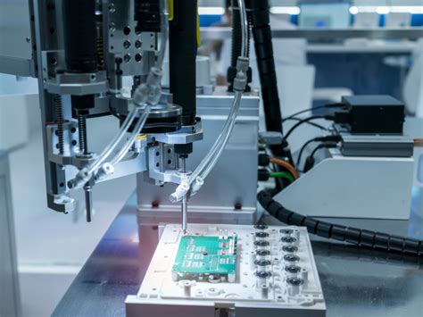
Automation in Modern PCB Manufacturing
The integration of automation into PCB assembly processes has revolutionized production efficiency and precision. Advanced robotic systems now handle tasks ranging from component placement to soldering, minimizing human error while accelerating throughput. For instance, PCBA (Printed Circuit Board Assembly) lines leverage pick-and-place machines with micron-level accuracy, ensuring consistent alignment of surface-mount devices (SMDs). Automated optical inspection (AOI) systems further enhance quality by scanning boards for defects like solder bridges or misaligned components in real time, reducing post-production rework.
Beyond hardware, software-driven workflows synchronize design data with manufacturing equipment, enabling seamless transitions from CAD files to physical boards. Machine learning algorithms analyze historical production data to optimize parameters such as solder paste application or reflow oven temperatures, adapting dynamically to varying PCB design complexities. This technological shift not only slashes turnaround times but also supports scalability for high-volume orders. Crucially, automation aligns with Design for Manufacturability (DFM) principles by flagging potential assembly challenges early, ensuring designs meet manufacturing-ready standards before reaching the factory floor.
As industries demand faster, more reliable PCBA solutions, the role of automation continues to expand—bridging the gap between innovative PCB design ambitions and economically viable, high-quality output.
Conclusion
In the realm of PCB design and manufacturing, achieving consistent quality demands a holistic approach that bridges innovation with precision. By prioritizing collaboration between design and production teams, organizations can address potential flaws in PCB assembly workflows before they escalate. Integrating DFM checks early in the process ensures that designs align with manufacturing capabilities, minimizing rework and delays. For PCBA (printed circuit board assembly) success, rigorous quality control protocols—such as automated optical inspection and functional testing—are indispensable to verify performance under real-world conditions.
Adopting data-driven strategies for material selection and process optimization further enhances reliability, particularly in high-frequency or high-temperature applications. As automation reshapes PCB manufacturing, leveraging advanced tools for traceability and error detection becomes critical to maintaining competitiveness. Ultimately, the convergence of meticulous design practices, robust DFM guidelines, and adaptive manufacturing frameworks forms the foundation for delivering circuit boards that meet evolving industry standards while balancing cost-efficiency and technical excellence.
FAQs
What are the critical factors for successful PCB assembly?
Effective PCB assembly relies on rigorous DFM checks, precise material compatibility, and adherence to thermal management guidelines. Proper solder mask application and component placement accuracy directly impact PCBA reliability.
How does material selection influence PCB performance?
Materials determine signal integrity, thermal resistance, and mechanical stability. High-frequency applications require low-loss dielectrics, while industrial environments demand flame-retardant substrates. Always align choices with operational requirements and manufacturing capabilities.
Why are automated optical inspections (AOI) essential in production?
AOI systems detect soldering defects, component misalignment, and trace imperfections with micron-level precision. This step reduces PCBA failure rates by 40–60% in high-volume manufacturing workflows.
What distinguishes PCB design from PCBA development?
PCB design focuses on layout and electrical connectivity, while PCBA encompasses component procurement, soldering, and functional testing. Both stages require synchronized collaboration between design and manufacturing teams.
Can prototyping reduce long-term production costs?
Yes. Prototyping identifies design flaws early, minimizing post-production rework. Iterative testing of PCB assembly processes optimizes yield rates and material usage, lowering per-unit costs by up to 30%.
How do environmental standards affect manufacturing workflows?
Compliance with RoHS and IPC-A-610 mandates lead-free soldering, halogen-free substrates, and waste management protocols. These standards ensure PCBA durability while meeting global regulatory requirements.
What role does thermal analysis play in reliability?
Simulating heat dissipation patterns prevents hotspots and component degradation. Techniques like finite element analysis (FEA) validate thermal vias and heatsink placements, extending PCB assembly lifespan in high-power applications.
Ready to Optimize Your PCB Assembly Process?
Please click here to explore tailored PCBA solutions and technical support: https://www.andwinpcb.com/pcb-assembly/.