Annular Ring in PCB Design: Importance, Calculation, and Best Practices
Introduction
Printed Circuit Boards (PCBs) are the backbone of modern electronics, providing mechanical support and electrical connections for components. One critical aspect of PCB design is ensuring proper plating and connectivity in drilled holes, particularly vias and plated through-holes (PTHs). The annular ring plays a vital role in maintaining the structural and electrical integrity of these connections.
This article explores the concept of the annular ring in PCB design, its significance, calculation methods, manufacturing considerations, and best practices to ensure reliability in electronic assemblies.
What is an Annular Ring?
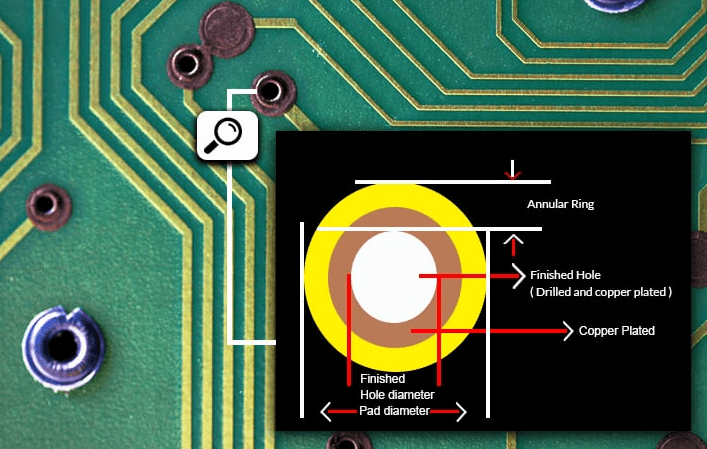
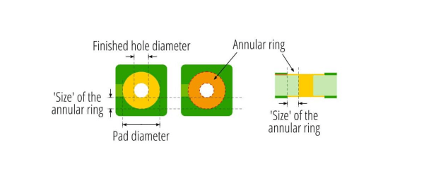
The annular ring refers to the copper pad area surrounding a drilled hole in a PCB. It is the conductive material that remains after drilling and plating, forming a critical connection point between the hole and the surrounding copper trace or plane.
Key Definitions:
- Drill Hole (Finished Hole Size): The final diameter of the hole after plating.
- Pad Diameter: The total diameter of the copper pad around the hole.
- Annular Ring Width: The distance from the edge of the drilled hole to the edge of the pad.
The formula for calculating the annular ring width is:
[
\text{Annular Ring Width} = \frac{(\text{Pad Diameter} – \text{Drill Hole Diameter})}{2}
]
A sufficient annular ring ensures proper electrical connectivity and mechanical strength, while an insufficient one can lead to manufacturing defects or reliability issues.
Importance of Annular Ring in PCB Design
1. Electrical Connectivity
The annular ring provides the conductive path between the plated hole and the surrounding copper. If the ring is too narrow, it may lead to weak connections or open circuits.
2. Mechanical Strength
Adequate annular ring width ensures that the via or PTH can withstand mechanical stresses during assembly (e.g., soldering, thermal cycling).
3. Manufacturing Tolerances
PCB fabrication involves drilling tolerances and misalignment. A wider annular ring compensates for slight drill shifts, preventing breakout (where the drill hole extends beyond the pad).
4. Signal Integrity (for High-Speed PCBs)
In high-frequency designs, insufficient annular rings can cause impedance mismatches, leading to signal reflections and degraded performance.
Annular Ring Standards and Industry Requirements
Different PCB manufacturers and industry standards define minimum annular ring requirements. Some key standards include:
- IPC-2221/7351: Recommends a minimum annular ring of 0.05mm (2 mils) for standard PCBs and 0.025mm (1 mil) for high-density designs.
- IPC Class 2 (General Electronics): Requires at least 0.025mm (1 mil) annular ring.
- IPC Class 3 (High-Reliability, Aerospace, Medical): Demands stricter tolerances, often 0.05mm (2 mils) or more.
Typical Annular Ring Values
| Application | Minimum Annular Ring Width |
|---|---|
| Standard PCB | 0.05mm (2 mils) |
| HDI (High-Density Interconnect) | 0.025mm (1 mil) |
| High-Power/High-Current | 0.1mm (4 mils) or more |
| RF/Microwave PCBs | 0.075mm (3 mils) |
Calculating Annular Ring in PCB Design
To ensure manufacturability, designers must calculate the annular ring based on drill size and pad diameter.
Example Calculation:
- Pad Diameter: 0.6mm
- Drill Hole Diameter: 0.3mm
- Annular Ring Width:
[\frac{(0.6 – 0.3)}{2} = 0.15 \text{mm (6 mils)}]
This provides a robust annular ring, well above the IPC minimum.
Accounting for Drill Tolerance & Misalignment
Manufacturing variations (e.g., drill wander, registration errors) can reduce the effective annular ring. A safety margin is recommended:
[\text{Effective Annular Ring} = \text{Calculated Width} – \text{Drill Tolerance}]
Common Annular Ring Defects and How to Avoid Them
1. Breakout (Drill Misalignment)
- Cause: Drilling inaccuracy shifts the hole outside the pad.
- Solution: Increase pad size or use smaller drill tolerances.
2. Insufficient Copper (Over-Etching)
- Cause: Excessive etching reduces copper thickness.
- Solution: Ensure proper etch compensation in fabrication.
3. Thermal Stress Cracks
- Cause: Poor annular ring leads to cracked vias during soldering.
- Solution: Use teardrop-shaped pads for better stress distribution.
Best Practices for Annular Ring Design
- Follow IPC Standards: Adhere to minimum annular ring requirements based on PCB class.
- Use Larger Pads for High-Current Traces: Wider annular rings improve current-carrying capacity.
- Optimize for HDI PCBs: Laser-drilled microvias require precise annular ring control.
- Simulate Manufacturing Tolerances: Account for drill shift in high-density designs.
- Apply Teardrops: Strengthen connections between traces and pads.
Conclusion
The annular ring is a fundamental aspect of PCB design, impacting electrical performance, manufacturability, and reliability. By understanding its importance, calculating appropriate widths, and following best practices, designers can ensure robust and high-quality PCB assemblies.
As PCB technology advances (e.g., HDI, flex circuits), annular ring optimization will remain critical for next-generation electronics. Always consult fabrication guidelines and perform Design for Manufacturability (DFM) checks to avoid costly defects.