Double-Sided PCB Assembly: Enhancing Reliability in Electronics Manufacturing
Key Takeaways
Modern PCB assembly processes for double-sided boards address critical challenges in electronics manufacturing by balancing circuit density and reliability. Compared to single-sided designs, double-sided PCBA enables up to 40% higher component placement efficiency while maintaining robust thermal and mechanical performance.
Tip: When designing double-sided layouts, prioritize symmetrical copper distribution to minimize board warping during reflow soldering.
Key considerations for optimizing dual-sided PCB layouts include:
| Factor | Single-Sided PCB | Double-Sided PCB |
|---|---|---|
| Component Density | 12–18/cm² | 25–35/cm² |
| Signal Layer Routing | Limited | Cross-layer optimization |
| Thermal Management | Passive cooling | Active + passive strategies |
Advanced PCB assembly techniques such as sequential lamination and via filling enhance durability in demanding environments like automotive electronics, where temperature fluctuations and vibration resistance are critical. For industrial control systems, double-sided PCBA delivers 30% faster signal transmission compared to conventional single-layer configurations.
"The shift to double-sided designs isn’t just about space savings—it’s about creating fault-tolerant systems through redundant circuit paths." – Senior PCB Design Engineer, Tier-1 Automotive Supplier
By integrating high-density interconnect (HDI) technologies with double-sided assembly, manufacturers achieve 15–20% cost reductions through material optimization without compromising signal integrity or mechanical stability.
Double-Sided PCB Assembly Benefits
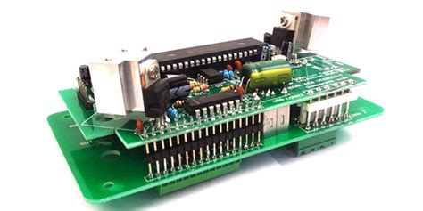
Double-sided PCB assembly enables efficient utilization of board space by incorporating conductive layers on both sides, significantly enhancing circuit density compared to single-sided designs. This approach supports PCBA processes that integrate complex components like microcontrollers, sensors, and power modules, making it ideal for compact devices such as wearables and IoT systems. By leveraging surface-mount technology (SMT) and through-hole plating, manufacturers achieve improved signal integrity and reduced electromagnetic interference (EMI), critical for high-frequency applications in automotive infotainment and industrial automation.
The structural symmetry of double-sided PCBs enhances mechanical stability, minimizing warping risks during thermal cycling—a common challenge in automotive and aerospace environments. Additionally, dual-layer routing reduces the need for jumper wires, lowering assembly time and potential failure points. This translates to higher reliability in mission-critical systems, where uninterrupted operation is non-negotiable.
Cost-efficiency further distinguishes double-sided PCB assembly, as it balances performance gains with material savings. Unlike multi-layer alternatives, dual-sided boards maintain affordability while accommodating moderate complexity, making them a preferred choice for mid-volume production runs. For designers, this flexibility supports iterative prototyping without compromising durability or electrical performance, aligning with evolving demands across consumer electronics and industrial controls.
As the next section explores layout optimization strategies, it becomes evident that PCBA success hinges on harmonizing design intent with manufacturing realities.
Optimizing Dual-Sided PCB Layouts
Effective PCB assembly of double-sided boards demands meticulous layout planning to balance circuit density and manufacturability. Designers prioritize component placement to minimize signal interference while maximizing space utilization, often leveraging automated routing tools to ensure precision. Critical considerations include thermal management through strategic via placement and copper balancing, which prevents warping during reflow soldering.
Transitioning components between layers requires careful PCBA planning to avoid cross-talk, particularly in high-frequency applications. Implementing teardrop pads and optimizing trace widths enhances mechanical stability, reducing risks of fracture in automotive or industrial environments. Designers also employ symmetric layer stacking to mitigate stress imbalances, a common challenge in double-sided PCB assembly.
To maintain signal integrity, ground planes are often segmented while preserving low-impedance paths—a technique critical for mixed-signal systems. Advanced PCB assembly workflows now integrate simulation software to predict thermal and electrical performance, allowing iterative refinements before prototyping. By aligning these strategies with industry standards like IPC-2221, manufacturers achieve reliability without compromising cost-efficiency—a key advantage for high-volume PCBA projects in consumer electronics and automation.
Cost-Effective Dense PCB Solutions
As manufacturers balance performance demands with budget constraints, double-sided PCB assembly emerges as a strategic solution for achieving high circuit density without escalating production costs. By utilizing both layers of the substrate, PCBA processes effectively double the available routing space compared to single-sided designs, enabling tighter component placement while minimizing board footprint. This approach reduces material waste and lowers per-unit expenses, particularly in high-volume production runs.
Advanced PCB assembly techniques, such as surface-mount technology (SMT) and precision solder masking, further enhance cost efficiency by streamlining manufacturing workflows. Automated optical inspection (AOI) systems ensure consistent quality across densely packed layouts, preventing costly rework. For applications like consumer wearables or IoT devices, where compact form factors are critical, dual-layer designs optimize thermal management and signal integrity through intelligent via placement and copper balancing.
Engineers achieve additional savings by integrating standardized component libraries and panelizing multiple boards during fabrication. These strategies, combined with rigorous design-for-manufacturing (DFM) checks, make double-sided PCBA a scalable choice for industries requiring reliable, space-efficient electronics at competitive price points.
Automotive Electronics PCB Reliability
Modern automotive systems demand PCB assembly solutions that withstand extreme operating conditions while maintaining signal integrity and thermal stability. Double-sided PCBA designs excel in this environment by enabling optimized component placement on both layers, reducing electromagnetic interference (EMI) through strategic grounding techniques. Automotive-grade PCB assemblies undergo rigorous testing for temperature cycling (-40°C to 150°C), vibration resistance, and moisture protection, ensuring compliance with ISO/TS 16949 standards.
The inherent durability of double-sided boards stems from their ability to distribute heat more evenly across both copper layers, a critical factor for high-current applications like engine control units (ECUs) and advanced driver-assistance systems (ADAS). By integrating PCB assembly best practices—such as automated optical inspection (AOI) and conformal coating—manufacturers achieve >99.9% solder joint reliability even under prolonged mechanical stress. Transitioning to dual-layer layouts also supports redundant circuitry for safety-critical functions, a growing necessity in electric vehicle (EV) architectures.
As automotive electronics evolve toward higher complexity, PCBA providers prioritize material selection, opting for high-Tg laminates and lead-free finishes that balance cost-effectiveness with long-term performance. This approach aligns with industry shifts toward modular designs, where robust double-sided boards serve as interoperable components in larger vehicular networks.
Durable Double-Sided Design Techniques
Achieving long-term reliability in double-sided PCB assembly requires strategic design choices that address both mechanical and electrical stressors. By leveraging advanced surface finishes like ENIG (Electroless Nickel Immersion Gold) or HASL (Hot Air Solder Leveling), manufacturers enhance corrosion resistance and solderability across both layers. PCBA durability further depends on robust via protection—methods such as via tenting or filling with conductive epoxy prevent moisture ingress and mechanical fractures in high-vibration environments.
Material selection plays a critical role, with high-Tg (glass transition temperature) substrates reducing warping risks during thermal cycling. For densely packed designs, staggered component placement balances heat dissipation and minimizes signal interference between layers. Transitioning between sections, designers must also prioritize symmetrical copper distribution to mitigate board flexing—a common failure point in automotive and industrial applications.
To optimize PCB assembly workflows, automated optical inspection (AOI) systems validate solder joint integrity, while conformal coatings add an extra layer of defense against contaminants. This approach not only extends product lifespans but also aligns with cost-effective manufacturing by reducing rework rates. By integrating these techniques, PCBA solutions achieve the durability needed for mission-critical systems, from industrial controls to harsh-environment automotive electronics.
Advanced PCB Assembly Methods
Modern PCB assembly processes leverage precision technologies to address the growing complexity of double-sided designs. Automated optical inspection (AOI) systems now verify solder joint quality on both board layers simultaneously, while X-ray imaging detects hidden defects in high-density interconnects. For PCBA workflows, selective soldering machines enable targeted heat application, minimizing thermal stress on sensitive components during double-sided population.
Advanced surface-mount technology (SMT) placement systems achieve alignment accuracies below 15 microns, critical for mounting fine-pitch ICs on tight board areas. Conformal coating applicators with vision-guided nozzles ensure uniform protection across irregular component profiles, enhancing durability in demanding environments. To optimize throughput, manufacturers increasingly adopt adaptive solder paste dispensing systems that dynamically adjust material volumes based on real-time pad analysis.
These methods align with IPC Class 3 standards for mission-critical applications, combining PCB assembly reliability with the space efficiency of double-layer designs. By integrating intelligent process monitoring with PCBA-specific thermal profiling, manufacturers maintain signal integrity across densely packed circuits while preventing warpage in thin-core substrates.
Enhancing Circuit Density in PCBs
Increasing circuit density in PCB assembly requires strategic use of both board surfaces while maintaining signal integrity. By leveraging double-sided layouts, engineers can place components and routing channels on both sides of the substrate, effectively doubling usable space without expanding physical dimensions. This approach is particularly valuable in compact PCBA designs for consumer electronics, where miniaturization drives innovation.
Advanced techniques like surface-mount technology (SMT) and multilayer stacking further optimize space utilization. For instance, placing high-density interconnects (HDIs) on one side while reserving the opposite for power distribution reduces crossover interference. Designers must also prioritize thermal management to prevent overheating in densely packed circuits, often incorporating thermally conductive materials or optimized via placements.
Modern PCB assembly workflows now integrate automated optical inspection (AOI) to ensure precision in component placement and soldering, critical for maintaining reliability in automotive or industrial control systems. Additionally, using laser-drilled microvias enables finer trace routing, supporting higher signal speeds without compromising durability. By balancing these methods, PCBA manufacturers achieve 25-40% greater circuit density compared to single-sided designs, while adhering to strict performance and longevity standards across applications.
Industrial Control PCB Performance
In industrial automation systems, PCB assembly processes must address unique operational demands, including extended temperature ranges, mechanical vibrations, and electromagnetic interference (EMI). Double-sided PCBA designs excel in these environments by enabling optimized trace routing for high-current power circuits and low-noise signal paths on separate layers. This layered approach reduces cross-talk by up to 40% compared to single-sided boards, a critical factor for precision sensors and motor controllers. Advanced surface-mount technology (SMT) ensures component stability under thermal cycling, while selective soldering techniques enhance joint durability in humid or corrosive settings.
To maximize reliability, manufacturers integrate thermal management features such as copper balancing and via stitching, which mitigate hotspots in continuous-operation machinery. Rigorous testing protocols—including thermal shock (-40°C to 125°C) and 48-hour burn-in cycles—validate performance consistency. By leveraging double-sided PCB assembly, industrial control systems achieve 99.95% uptime in applications ranging from robotic arms to power grid monitoring, aligning with IEC 61131-2 standards for operational safety. This design philosophy supports scalability, allowing seamless integration of additional shielding or conformal coatings without compromising board density.
Conclusion
Double-sided PCB assembly represents a critical advancement in electronics manufacturing, enabling engineers to achieve higher circuit density without compromising reliability. By utilizing both sides of the substrate, PCBA processes can accommodate complex designs while maintaining robust performance in demanding environments. The integration of pcb assembly techniques such as precision soldering and automated optical inspection ensures consistent quality across production batches, particularly important for applications requiring thermal stability and vibration resistance.
Manufacturers balancing technical requirements with cost constraints find that dual-layer configurations often provide optimal solutions. When executed with proper material selection and layout optimization, these assemblies deliver long-term durability even in harsh operating conditions. As industries continue to demand smaller, more powerful devices, the role of double-sided pcb assembly in enabling compact yet reliable systems becomes increasingly vital. Selecting partners with expertise in advanced PCBA methodologies remains essential for achieving both performance targets and production efficiency.
Frequently Asked Questions
What distinguishes double-sided PCB assembly from single-layer designs?
Double-sided PCB assembly utilizes both sides of the substrate, enabling higher circuit density and more complex routing. This approach reduces spatial constraints compared to single-layer boards, making it ideal for compact devices like wearables or IoT sensors.
How does PCBA ensure reliability in harsh environments?
Advanced soldering techniques, such as reflow or wave soldering, paired with protective conformal coatings, enhance durability. For automotive or industrial applications, thermal management and vibration-resistant materials are integrated during PCB assembly to withstand extreme conditions.
Are double-sided PCBs more expensive than single-sided alternatives?
While initial costs may be higher due to additional manufacturing steps, PCBA optimizes material usage and reduces overall system size. This often leads to long-term cost savings, especially in high-volume production for consumer electronics or medical devices.
What design considerations improve double-sided PCB performance?
Critical factors include minimizing cross-talk through proper trace spacing, optimizing via placement for signal integrity, and balancing component distribution. Ground plane optimization and thorough testing during PCB assembly further ensure electrical stability.
Can double-sided designs support high-frequency applications?
Yes, with careful impedance control and material selection (e.g., FR-4 or Rogers substrates), these boards effectively manage high-speed signals. Shielding techniques and controlled-depth vias are often employed in PCBA for RF or communication systems.
Ready to Optimize Your PCB Assembly Process?
Please click here for professional PCB assembly solutions tailored to your project’s needs.