Coil on PCB: Design, Applications, and Advancements
Introduction
Printed Circuit Boards (PCBs) are widely used in modern electronics for interconnecting components and providing mechanical support. One of the emerging applications of PCBs is the integration of coils directly onto the board, known as Coil on PCB. These embedded coils serve various functions, including inductive sensing, wireless power transfer, RF communication, and electromagnetic interference (EMI) suppression.
This article explores the design considerations, manufacturing techniques, applications, and future trends of Coil on PCB technology.
1. What is a Coil on PCB?
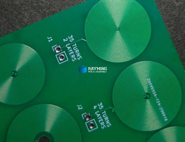
A Coil on PCB refers to a spiral or helical conductive trace fabricated on a printed circuit board to function as an inductor, transformer, or antenna. Unlike traditional wire-wound coils, PCB-based coils are etched using standard PCB manufacturing processes, offering better precision, repeatability, and integration with other electronic components.
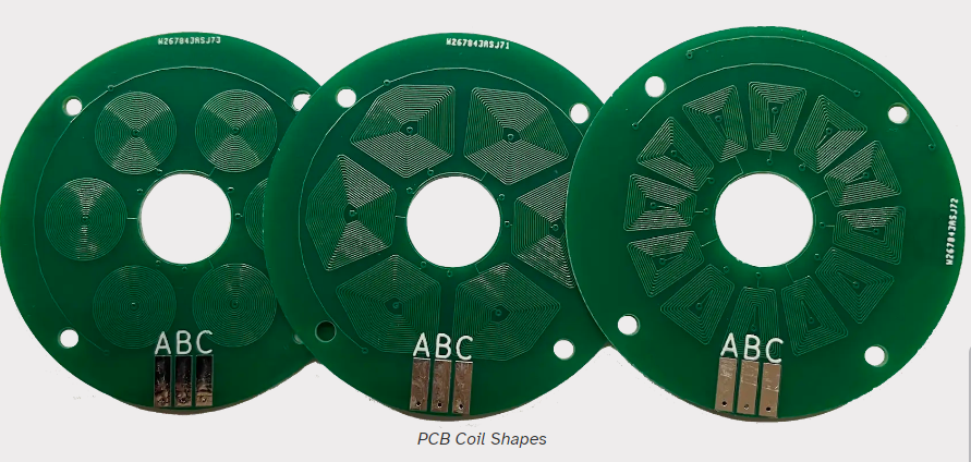
Types of Coils on PCB
- Single-layer coils: Simple spiral traces on one PCB layer.
- Multi-layer coils: Stacked spirals across multiple layers for higher inductance.
- Planar transformers: Multiple interconnected coils for power conversion.
- RF antennas: Used in near-field communication (NFC), RFID, and wireless charging.
2. Design Considerations for Coil on PCB
2.1 Inductance Calculation
The inductance of a PCB coil depends on:
- Number of turns (N)
- Trace width and spacing
- Inner and outer diameters
- PCB material (dielectric constant)
The modified Wheeler formula is commonly used for planar spiral inductance estimation:
[
L = \frac{\mu_0 N^2 d_{avg}}{2} \left( \ln{\left( \frac{2.46}{\rho} \right)} + 0.2 \rho^2 \right)
]
Where:
- ( L ) = Inductance (H)
- ( \mu_0 ) = Permeability of free space
- ( d_{avg} ) = Average diameter of the coil
- ( \rho ) = Fill ratio (inner diameter / outer diameter)
2.2 Trace Width and Spacing
- Wider traces reduce resistance (lower DC losses).
- Narrower spacing increases inductance but may cause manufacturing challenges.
- Skin effect at high frequencies must be considered.
2.3 Layer Stackup
- Multi-layer PCBs allow for higher inductance by connecting coils in series.
- Via placement affects parasitic capacitance and resistance.
2.4 Substrate Material
- FR-4 is common but has high dielectric losses at high frequencies.
- Rogers or polyimide substrates are better for RF applications.
3. Manufacturing Techniques
3.1 PCB Fabrication Process
- Copper etching: Spiral traces are patterned using photolithography.
- Via drilling and plating: For multi-layer coil connections.
- Solder mask application: Protects the coil from oxidation.
3.2 Advanced Techniques
- Embedded coils: Using laser direct structuring (LDS) for 3D integration.
- Flexible PCBs: For wearable and bendable coil applications.
- Additive manufacturing: 3D printing of conductive traces for custom geometries.
4. Applications of Coil on PCB
4.1 Wireless Power Transfer (WPT)
- Qi wireless charging (smartphones, wearables).
- Medical implants (low-power inductive coupling).
4.2 Inductive Sensing
- Proximity sensors (touchless switches).
- Metal detection (industrial automation).
4.3 RF Communication
- NFC and RFID antennas (contactless payments, access control).
- IoT devices (low-power wireless communication).
4.4 EMI Suppression
- Common-mode chokes to filter noise in high-speed circuits.
4.5 Planar Transformers
- DC-DC converters (miniaturized power supplies).
5. Advantages and Challenges
5.1 Advantages
✅ Compact and lightweight – No bulky wire windings.
✅ High precision – Consistent manufacturing tolerances.
✅ Integration with electronics – No additional assembly steps.
✅ Scalability – Easy to mass-produce.
5.2 Challenges
❌ Limited inductance compared to traditional coils.
❌ Higher AC resistance due to skin effect.
❌ Thermal management – Heat dissipation in high-current applications.
6. Future Trends
6.1 Higher-Frequency Applications
- 5G and mmWave demand advanced PCB coil designs.
6.2 Integration with Flexible Electronics
- Stretchable coils for biomedical and wearable tech.
6.3 AI-Optimized Coil Designs
- Machine learning algorithms for optimizing trace geometry.
6.4 Sustainable Manufacturing
- Recyclable PCBs with eco-friendly materials.
7. Conclusion
Coil on PCB technology is a versatile solution for modern electronics, enabling compact, high-performance inductive components. While challenges like limited inductance and thermal issues persist, advancements in materials, manufacturing, and AI-driven design are expanding its applications.
As wireless power, IoT, and high-frequency communication grow, Coil on PCB will play an increasingly critical role in next-generation electronic systems.