The Bed of Nails Tester: A Comprehensive Overview

Introduction to Bed of Nails Testing

In the world of printed circuit board (PCB) manufacturing and testing, the bed of nails tester has established itself as an essential tool for quality assurance and production efficiency. This specialized testing fixture, named for its resemblance to the ancient torture device, provides a reliable and efficient method for testing PCBs at various stages of production.

A bed of nails tester is essentially a test fixture that consists of an array of spring-loaded pogo pins arranged to match the test points on a specific PCB design. When the board is pressed onto this “bed,” the pins make electrical contact with predetermined test points, allowing for comprehensive electrical testing without the need for manual probing.

Historical Development

The concept of bed of nails testing emerged in the 1960s as electronics manufacturing began to scale up and the need for efficient testing methods became apparent. Early versions were simple fixtures with manually arranged nails, but as PCBs grew more complex, so did the testing systems.

The 1980s saw significant advancements with the introduction of computer-controlled systems that could automatically program test sequences and analyze results. Modern bed of nails testers now incorporate sophisticated software, high-density pin arrangements, and advanced diagnostic capabilities that were unimaginable in the early days of PCB testing.

Components and Architecture

A typical bed of nails test system consists of several key components:

  1. Fixture Plate: The physical structure that holds the array of test pins in precise alignment with the PCB’s test points.
  2. Pogo Pins: Spring-loaded test probes that provide reliable electrical contact. These come in various sizes and configurations depending on the application requirements.
  3. Interface Hardware: The electronic components that connect the test pins to the test system’s measurement instruments.
  4. Test Controller: The computer system that manages test sequences, collects data, and analyzes results.
  5. Software Suite: Programs that allow test programming, result analysis, and data management.

Modern systems may also include additional features like optical inspection, boundary scan capabilities, and networked data collection for statistical process control.

Working Principle

The operation of a bed of nails tester follows a systematic process:

  1. Fixture Preparation: The test fixture is custom-built to match the specific PCB layout, with each test pin positioned to contact a designated test point on the board.
  2. Board Loading: The PCB is precisely aligned and pressed onto the fixture, either manually or through automated machinery.
  3. Contact Establishment: The spring-loaded pins make electrical contact with the board’s test points, pads, or through-holes.
  4. Test Execution: The system applies test signals and measures responses according to pre-programmed test routines.
  5. Result Analysis: The system compares measured values against expected parameters and flags any discrepancies.
  6. Board Removal: The tested PCB is removed from the fixture, with pass/fail indications typically provided immediately.

Types of Bed of Nails Testers

Several variations of bed of nails testers have been developed to address different testing needs:

  1. Universal Grid Testers: Feature a standard grid pattern that can be adapted to different boards using interchangeable probe modules.
  2. Dedicated Fixture Testers: Custom-built for specific PCB designs, offering the highest density and most reliable contact.
  3. Flying Probe Hybrids: Combine traditional bed of nails with movable probes for additional flexibility.
  4. In-Circuit Testers (ICT): Comprehensive systems that can test components and sub-circuits in addition to connectivity.
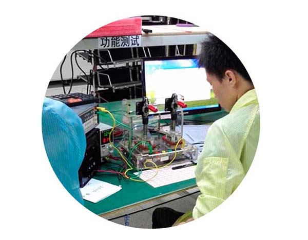
  5. Functional Testers: Designed to verify the complete functionality of the assembled PCB.

Advantages of Bed of Nails Testing

The widespread adoption of bed of nails testers in electronics manufacturing stems from several significant advantages:

  1. Speed: Capable of testing hundreds or thousands of points in seconds, far faster than manual probing.
  2. Repeatability: Provides consistent test conditions for every board tested.
  3. Comprehensiveness: Can access virtually all test points simultaneously for thorough testing.
  4. Reliability: Spring-loaded pins provide consistent pressure and reliable contact.
  5. Cost-Effectiveness: Despite initial fixture costs, the per-unit testing cost is very low for high-volume production.
  6. Automation Compatibility: Easily integrated into automated production lines.
  7. Diagnostic Capability: Can quickly identify specific faults for efficient repair.

Limitations and Challenges

While powerful, bed of nails testing does have some limitations:

  1. Fixture Costs: Custom fixtures can be expensive to design and manufacture, making them less economical for low-volume production.
  2. Physical Access Requirements: Requires dedicated test points on the PCB, which may conflict with miniaturization trends.
  3. Maintenance: Pins can wear out or become contaminated, requiring periodic replacement or cleaning.
  4. Limited Flexibility: Each fixture is typically designed for a specific PCB layout, requiring new fixtures for design changes.
  5. High-Density Challenges: Testing very fine-pitch components can be difficult due to physical constraints on pin size and spacing.

Design Considerations for Effective Testing

To maximize the effectiveness of bed of nails testing, several design factors must be considered:

  1. Test Point Placement: Strategic location of test points to ensure accessibility and coverage.
  2. PCB Layout: Considerations for fixture clearance and mechanical stability during testing.
  3. Pin Selection: Appropriate choice of pin types and sizes based on test point characteristics.
  4. Fixture Design: Mechanical design to ensure proper alignment and uniform pressure distribution.
  5. Test Coverage: Planning test sequences to achieve desired fault coverage while minimizing test time.

Applications in Modern Electronics Manufacturing

Bed of nails testers find application across various stages of electronics production:

  1. PCB Bare Board Testing: Verifying continuity and isolation before component population.
  2. In-Circuit Testing: Checking component values and basic functionality after assembly.
  3. Functional Testing: Verifying overall board operation before system integration.
  4. Quality Assurance: Final verification before shipment to customers.
  5. Repair and Rework: Diagnosing faults in returned or defective units.

Technological Advancements

Recent developments have enhanced bed of nails testing capabilities:

  1. Higher Density Probes: Miniature probes allowing testing of high-density boards with fine-pitch components.
  2. Advanced Materials: Improved probe materials for longer life and better contact reliability.
  3. Smart Fixtures: Fixtures with embedded electronics for better signal integrity and reduced cabling.
  4. Integrated Optical Inspection: Combining electrical testing with visual inspection capabilities.
  5. AI-Powered Diagnostics: Using machine learning to analyze test results and predict failure modes.

Comparison with Alternative Testing Methods

While bed of nails remains popular, alternative methods have emerged:

  1. Flying Probe Testers: Use movable probes instead of fixed arrays, offering flexibility but slower operation.
  2. Boundary Scan: Uses built-in test circuitry for digital components, but requires specific design features.
  3. AOI (Automated Optical Inspection): Good for visual defects but cannot detect electrical faults.

In practice, many manufacturers use a combination of these methods to achieve comprehensive test coverage.

Future Trends and Developments

The future of bed of nails testing includes several promising directions:

  1. Adaptive Fixtures: Configurable pin arrangements that can adapt to different board designs.
  2. Nanotechnology Probes: Ultra-fine probes for testing advanced packaging technologies.
  3. IoT Integration: Real-time monitoring and data analytics for predictive maintenance and process optimization.
  4. Enhanced Materials: New composite materials for probes with improved durability and conductivity.
  5. Hybrid Systems: Closer integration with other test methods for comprehensive quality assurance.

Best Practices for Implementation

To successfully implement bed of nails testing, manufacturers should:

  1. Involve test engineers early in the PCB design process
  2. Standardize test point locations where possible
  3. Establish regular fixture maintenance schedules
  4. Implement comprehensive test program verification
  5. Train operators thoroughly in fixture handling and test interpretation
  6. Continuously monitor test results for process improvement opportunities

Conclusion

The bed of nails tester remains a cornerstone of PCB manufacturing quality assurance despite the emergence of alternative testing methods. Its unparalleled combination of speed, reliability, and comprehensiveness ensures its continued relevance in an industry where quality and efficiency are paramount. As electronic devices continue to evolve, so too will bed of nails testing technology, adapting to meet the challenges of higher densities, more complex circuits, and ever-increasing quality demands.

For electronics manufacturers, investing in proper bed of nails test capabilities—whether in-house or through testing service providers—represents a critical step in ensuring product quality, reducing returns, and maintaining competitive advantage in the global marketplace. As we look to the future, the integration of smart technologies and advanced materials promises to extend the capabilities of this proven testing methodology well into the coming decades of electronics innovation.

Similar Posts