Key Factors for Reliable PCB Manufacturing and Assembly
Key Takeaways
Successful PCB assembly relies on balancing technical precision with systematic quality assurance. At its core, design considerations like trace spacing, component placement, and thermal relief patterns directly influence manufacturability and long-term reliability. Equally critical is material selection, where substrate quality, copper thickness, and solder mask type determine resistance to environmental stressors such as moisture or temperature fluctuations.
Tip: Prioritize IPC-6012 standards during design reviews to preemptively address potential assembly challenges.
Modern PCBA workflows demand advanced soldering techniques, including reflow and wave soldering, to maintain joint integrity across high-density layouts. Pairing these methods with automated optical inspection (AOI) ensures microscopic defect detection, reducing field failure risks. Additionally, thermal management strategies—such as via placement and heatsink integration—prevent overheating in mission-critical applications.
A reliable PCB assembly checklist should encompass design-for-manufacturability (DFM) validation, component traceability, and post-assembly functional testing. Transitioning between these phases requires seamless coordination between design and production teams to avoid costly rework.
By integrating robust testing protocols like in-circuit testing (ICT) and environmental stress screening (ESS), manufacturers can verify performance under real-world operating conditions. This systematic approach bridges the gap between theoretical design and durable electronics performance, ensuring PCBA outcomes meet both technical specifications and end-user expectations.

PCB Design Essentials for Reliability
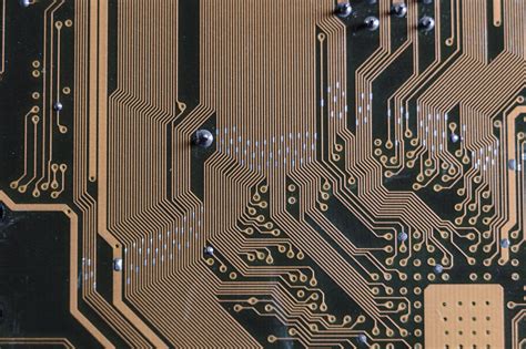
A robust PCB assembly process begins with foundational design principles that prioritize long-term functionality. Implementing design for manufacturing (DFM) guidelines ensures compatibility with automated PCBA workflows, reducing risks of mechanical stress or signal interference. Critical considerations include trace routing precision to minimize crosstalk, adequate spacing between high-voltage components, and strategic placement of vias to enhance thermal dissipation.
Layer stackup configuration plays a pivotal role in balancing signal integrity and mechanical stability, particularly in multi-layer boards. For instance, symmetrical copper distribution prevents warping during reflow soldering—a common challenge in PCB assembly. Additionally, incorporating thermal relief pads and teardrop transitions at component junctions mitigates solder joint fatigue, a frequent failure point in harsh operating environments.
Designers must also account for testability by integrating standardized test points compatible with automated inspection systems. This foresight streamlines post-assembly validation, aligning with the broader PCBA quality assurance framework. By addressing these elements early, engineers lay the groundwork for scalable production while ensuring compliance with industry standards like IPC-2221. Such proactive design choices not only enhance reliability but also reduce rework costs, creating a seamless transition to subsequent manufacturing stages.
Material Selection Impact on PCB Assembly
The choice of materials in PCB assembly directly influences the performance, durability, and manufacturability of the final product. Substrate materials, such as FR-4, polyimide, or ceramic-based laminates, determine thermal stability and electrical insulation, critical for high-frequency or high-temperature applications. For instance, PCBA designs requiring extended thermal cycling often utilize polyimide substrates due to their superior heat resistance.
Copper foil thickness and solder mask quality also play pivotal roles. Thicker copper layers (e.g., 2 oz vs. 1 oz) enhance current-carrying capacity but require precise soldering techniques to avoid bridging. Meanwhile, high-quality solder masks prevent oxidation and ensure consistent solder adhesion, reducing defects during reflow processes.
| Material Property | Impact on PCB Assembly |
|---|---|
| Substrate Dielectric Constant | Signal integrity in high-speed circuits |
| Copper Weight | Current handling & thermal dissipation |
| Solder Mask Adhesion | Solder joint reliability & contamination |
Thermal management materials, like thermally conductive adhesives or metal-core substrates, mitigate heat buildup in PCBA, extending component lifespan. Additionally, selecting halogen-free laminates aligns with environmental regulations without compromising mechanical strength. By balancing electrical, thermal, and mechanical properties, manufacturers optimize PCB assembly outcomes, ensuring compatibility with downstream processes like automated testing and final product integration.
Advanced Soldering Techniques for PCBs
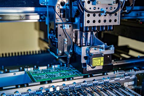
Effective PCB assembly relies heavily on precision soldering methods to ensure electrical connectivity and mechanical stability. Surface-mount technology (SMT) and through-hole technology (THT) remain foundational, but modern PCBA processes demand advanced approaches to address miniaturization and high-density designs. Reflow soldering, optimized for SMT components, employs controlled thermal profiles to melt solder paste uniformly, reducing voids or cold joints. For mixed-technology boards, selective soldering targets specific areas, minimizing thermal stress on sensitive components.
In high-reliability applications, techniques like vapor-phase soldering offer precise temperature control, while laser soldering provides micron-level accuracy for fine-pitch ICs or RF modules. Proper solder alloy selection—such as SAC305 for lead-free requirements—directly impacts joint durability under thermal cycling. Additionally, automated optical inspection (AOI) systems validate solder joint integrity, flagging issues like solder bridges or insufficient wetting.
To mitigate defects in PCB assembly, operators must balance process parameters, including flux chemistry, peak temperatures, and cooling rates. Advanced PCBA workflows also integrate nitrogen environments to reduce oxidation during soldering, enhancing joint reliability. These techniques, when paired with rigorous testing protocols, ensure robust interconnections critical for long-term electronics performance.
Testing Protocols Ensuring Electronics Durability
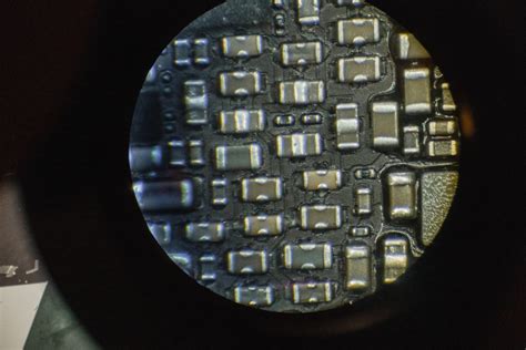
Robust PCB assembly processes rely on rigorous testing protocols to guarantee long-term performance in electronic devices. At the PCBA stage, comprehensive validation begins with automated optical inspection (AOI), which scans for soldering defects, component misalignment, or trace irregularities. In-circuit testing (ICT) follows, verifying electrical connectivity and identifying short circuits or open connections. For high-density boards, X-ray inspection becomes critical to assess hidden solder joints under ball grid arrays (BGAs) or multilayer configurations.
Environmental stress tests, such as thermal cycling and vibration resistance evaluations, simulate real-world operating conditions to ensure durability. These protocols align with industry standards like IPC-A-610 and ISO 9001, which define acceptability criteria for PCB assembly outcomes. Additionally, functional testing validates the assembled board’s performance against design specifications, confirming that power distribution, signal integrity, and firmware interactions meet operational demands.
By integrating these layered checks, manufacturers minimize latent failures and enhance product lifespan. Transitioning seamlessly from design validation to post-production audits, such protocols form the backbone of reliable PCBA workflows, ensuring electronics withstand both immediate and prolonged stressors.
Quality Control in PCB Manufacturing Processes
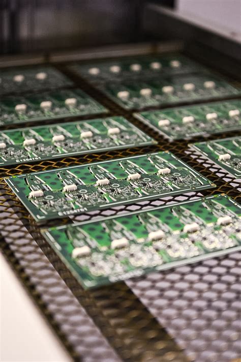
Effective PCB assembly relies on rigorous quality control measures to mitigate defects and ensure long-term reliability. During manufacturing, automated inspection systems like Automated Optical Inspection (AOI) and X-ray imaging validate solder joint integrity, layer alignment, and component placement accuracy. For PCBA (Printed Circuit Board Assembly), statistical process control (SPC) tracks critical parameters such as reflow oven temperature profiles and solder paste deposition consistency, reducing variability.
Material verification forms another cornerstone, with suppliers audited for compliance with industry standards like IPC-A-610 or ISO 9001. Cross-functional teams often employ Failure Mode and Effects Analysis (FMEA) to preemptively address risks in high-density or mixed-technology boards. Post-assembly, environmental stress testing—including thermal cycling and vibration simulations—confirms durability under real-world conditions.
Seamless integration of these protocols with PCB assembly workflows ensures defects are identified early, minimizing rework costs. Transitioning to subsequent stages, such as functional testing, becomes more efficient when upstream quality metrics are rigorously enforced. This systematic approach not only aligns with global reliability benchmarks but also supports downstream processes like thermal management and layout optimization.
Thermal Management Role in PCB Reliability
Effective thermal management is a cornerstone of reliable electronics performance in PCB assembly. As components shrink and power densities increase, managing heat dissipation becomes critical to prevent thermal stress—a leading cause of premature failure in PCBA. Designers must prioritize thermal vias, copper pours, and strategic component placement to channel heat away from sensitive areas. Materials with high thermal conductivity, such as metal-core substrates or advanced laminates, further enhance heat distribution.
During PCB assembly, soldering processes like reflow profiling must account for thermal expansion coefficients to avoid microcracks in joints. Post-assembly, thermal cycling tests validate a board’s resilience under fluctuating temperatures, ensuring long-term durability. Integrating heat sinks or active cooling solutions in the final PCBA design can mitigate hotspots, particularly in high-power applications.
Balancing these strategies not only extends product lifespans but also aligns with broader quality control frameworks, reinforcing the interdependence of thermal design and PCB reliability across manufacturing stages.
Optimizing PCB Layout for Assembly Success
Effective PCB assembly relies heavily on a well-optimized layout that balances design complexity with manufacturability. A critical first step involves strategic component placement to minimize signal interference and thermal hotspots while ensuring accessibility for PCBA processes. Grouping components with similar functions or thermal requirements reduces soldering challenges and streamlines automated pick-and-place workflows.
Equally critical is maintaining adequate spacing between high-density components to prevent solder bridging during reflow. For instance, fine-pitch ICs or connectors require precise pad geometries and solder mask alignment to avoid defects. Design for manufacturability (DFM) principles, such as standardizing pad sizes and avoiding asymmetrical footprints, further enhance compatibility with PCB assembly equipment.
Additionally, optimizing trace routing to avoid sharp angles or unnecessary vias improves signal integrity and reduces impedance mismatches. Incorporating test points and fiducial markers into the layout ensures reliable alignment for automated optical inspection (AOI) systems, a cornerstone of quality assurance in PCBA. By collaborating with fabrication partners early in the design phase, engineers can preemptively address issues like panelization constraints or material limitations, ensuring seamless transitions from prototyping to mass production.
Finally, validating the layout through simulation tools helps identify thermal expansion risks or mechanical stress points, safeguarding long-term reliability in demanding environments.

Reliable PCB Assembly Checklist Essentials
A systematic PCB assembly checklist is critical for minimizing defects and ensuring consistent performance in electronic devices. Building on design and material considerations, this checklist should prioritize design-for-manufacturability (DFM) validation to confirm component placement aligns with PCBA workflows. Verify material compatibility—such as solder paste viscosity and substrate thermal stability—to prevent delamination or warping during reflow soldering.
Next, inspect soldering techniques, including temperature profiles for reflow ovens and wave soldering parameters, to avoid cold joints or bridging. Incorporate automated optical inspection (AOI) and X-ray testing to detect hidden flaws like voids or misaligned BGA components. Post-assembly, functional testing under simulated operating conditions—such as thermal stress cycles or vibration tests—ensures reliability in real-world applications.
Finally, document traceability metrics, including batch numbers for critical components and solder paste expiration dates, to streamline quality audits. By integrating these steps into a standardized PCB assembly protocol, manufacturers reduce rework costs and enhance product longevity, aligning with broader goals of electronics durability outlined in earlier sections.
Conclusion
Achieving reliability in PCB assembly requires a holistic approach that integrates design foresight, material precision, and process control. As discussed, factors like thermal management, solder joint integrity, and automated optical inspection (AOI) play pivotal roles in ensuring durable PCBA outcomes. Manufacturers must balance design-for-manufacturability (DFM) principles with rigorous testing protocols to mitigate risks such as signal interference or component degradation.
Transitioning from prototyping to full-scale production demands adherence to industry standards (e.g., IPC-A-610), coupled with real-time data analytics to refine PCB assembly workflows. The interplay between high-quality substrates and advanced soldering techniques—such as reflow or selective soldering—directly impacts long-term performance in harsh environments.
Ultimately, reliability hinges on a closed-loop quality system that validates every stage, from layout optimization to final PCBA validation. By prioritizing traceability and failure mode analysis, stakeholders can preemptively address vulnerabilities, ensuring electronics meet both functional and endurance expectations. This systematic alignment of design, materials, and process expertise remains the cornerstone of trustworthy PCB manufacturing and assembly.
Frequently Asked Questions
What distinguishes PCB assembly from PCBA?
PCB assembly refers to the process of populating a bare circuit board with components, while PCBA (Printed Circuit Board Assembly) represents the fully assembled and functional unit. The terms are often used interchangeably, but PCBA specifically emphasizes the completed product ready for integration into devices.
How does material selection impact PCB assembly reliability?
High-quality substrates, copper layers, and solder masks prevent delamination and thermal stress. For example, using FR-4-grade laminates ensures stability in high-temperature environments, while lead-free solder alloys enhance durability. Poor material choices can lead to premature failure during PCBA operation.
What testing protocols are critical for reliable PCB assembly?
Automated Optical Inspection (AOI), X-ray testing, and In-Circuit Testing (ICT) identify soldering defects, component misalignment, and electrical faults. Environmental stress screening (ESS) further validates performance under extreme conditions, ensuring long-term reliability for PCBA units.
Why is thermal management vital in PCB assembly?
Excessive heat degrades components and solder joints. Techniques like thermal vias, heatsinks, and proper trace spacing dissipate heat efficiently. Neglecting this can shorten the lifespan of PCBA systems, especially in high-power applications.
How can design errors affect PCB assembly outcomes?
Inadequate clearances, improper pad sizes, or mismatched footprints lead to soldering defects or component damage. Collaboration between design and PCB assembly teams ensures manufacturability, reducing rework costs and delays.
Explore Professional PCB Assembly Solutions
For tailored guidance on optimizing your PCBA projects, please click here to connect with industry experts and access advanced manufacturing resources.