ENIG PCB Finish: A Comprehensive Guide
Introduction to ENIG PCB Finish
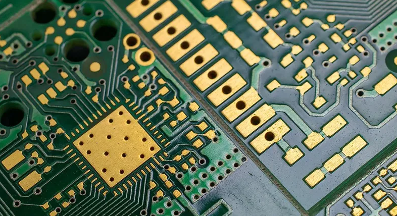
Electroless Nickel Immersion Gold (ENIG) has become one of the most popular surface finishes in the printed circuit board (PCB) industry. This two-layer metallic coating combines the benefits of nickel’s excellent barrier properties with gold’s superior conductivity and oxidation resistance. ENIG provides a flat, solderable surface that is ideal for fine-pitch components and offers excellent shelf life compared to other finishes.
The ENIG process involves depositing a thin layer of nickel-phosphorus alloy through an autocatalytic chemical reaction, followed by a thin layer of gold deposited via a displacement reaction. This combination creates a robust surface that protects the underlying copper from oxidation while maintaining excellent electrical connectivity. Since its introduction in the 1990s, ENIG has gained widespread adoption across various industries, including telecommunications, aerospace, medical devices, and consumer electronics.
The ENIG Process: Step-by-Step
1. Surface Preparation
The ENIG process begins with thorough cleaning of the PCB surface to remove any contaminants, oxides, or residues from previous manufacturing steps. This typically involves:
- Alkaline cleaning to remove organic contaminants
- Microetching to remove surface oxides and provide texture
- Acid rinsing to neutralize any remaining alkaline solutions
2. Electroless Nickel Deposition
The cleaned copper surface is then immersed in an electroless nickel plating bath containing:
- Nickel ions (typically nickel sulfate)
- A reducing agent (usually sodium hypophosphite)
- Complexing agents to control deposition rate
- Stabilizers to prevent spontaneous decomposition
- pH adjusters and buffers
The nickel deposits autocatalytically on the copper surface through the following reaction:
Ni²⁺ + H₂PO₂⁻ + H₂O → Ni⁰ + H₂PO₃⁻ + 2H⁺
This process creates a uniform nickel-phosphorus alloy layer typically 3-6 μm thick with phosphorus content between 7-11%.
3. Immersion Gold Deposition
After nickel deposition, the board is rinsed and transferred to the immersion gold bath, which contains:
- Gold ions (typically from potassium gold cyanide)
- Complexing agents
- pH buffers
- Temperature control agents
The gold deposition occurs through a displacement reaction where nickel atoms oxidize and dissolve while gold ions reduce and deposit:
Ni⁰ + 2Au⁺ → Ni²⁺ + 2Au⁰
The resulting gold layer is typically 0.05-0.15 μm thick—just enough to protect the nickel from oxidation while maintaining excellent solderability.
Advantages of ENIG Finish
1. Excellent Surface Planarity
ENIG provides an exceptionally flat surface, making it ideal for:
- Fine-pitch components (including QFNs and BGAs)
- High-density interconnect (HDI) designs
- Surface mount technology (SMT) assembly
2. Superior Solderability
The gold layer protects the nickel from oxidation while:
- Providing excellent wetting for solder
- Maintaining consistent solder joint formation
- Allowing for multiple reflow cycles
3. Long Shelf Life
ENIG-finished PCBs can typically be stored for:
- 12 months or more in proper conditions
- Without significant degradation in solderability
- Compared to 3-6 months for OSP or HASL finishes
4. Compatibility with Various Technologies
ENIG works well with:
- Lead-free soldering processes
- Wire bonding (especially for gold wires)
- Press-fit connectors
- Mixed technology assemblies
5. Reliable Electrical Performance
The finish provides:
- Low contact resistance
- Stable impedance characteristics
- Good high-frequency performance
Challenges and Limitations of ENIG
1. Black Pad Syndrome
One of the most notorious issues with ENIG is black pad, characterized by:
- Darkened nickel surfaces under the gold layer
- Weak or brittle solder joints
- Potential for catastrophic failure under stress
Causes include:
- Over-accelerated nickel deposition
- Contaminated nickel baths
- Improper gold immersion process
2. Higher Cost Compared to Alternatives
ENIG is more expensive than:
- HASL (Hot Air Solder Leveling)
- OSP (Organic Solderability Preservative)
- Immersion tin or silver
3. Process Complexity
ENIG requires:
- Strict process control
- Frequent bath analysis and maintenance
- Skilled operators
- Specialized equipment
4. Limited Thickness Options
The immersion gold process has natural limitations on thickness:
- Too thin (<0.05 μm) may not provide adequate protection
- Too thick (>0.15 μm) can lead to embrittlement
- Not suitable for heavy gold requirements (>0.25 μm)
ENIG vs. Other PCB Finishes
1. ENIG vs. HASL
- ENIG is flatter and better for fine-pitch components
- HASL is cheaper but has uneven surfaces
- ENIG is lead-free by nature; HASL may contain lead
2. ENIG vs. OSP
- ENIG has longer shelf life
- OSP is cheaper but less durable
- ENIG better for multiple reflow cycles
3. ENIG vs. Immersion Silver
- Silver is cheaper but tarnishes more easily
- ENIG has better shelf life
- Silver may have better high-frequency performance
4. ENIG vs. ENEPIG
- ENEPIG (Electroless Nickel Electroless Palladium Immersion Gold) adds a palladium layer
- ENEPIG is more expensive but better for wire bonding
- ENEPIG has reduced risk of black pad
Applications of ENIG Finish
1. High-Reliability Electronics
- Aerospace and defense systems
- Medical devices
- Automotive electronics (especially under-hood applications)
2. Fine-Pitch Components
- BGA packages
- QFN components
- High-density interconnects
3. RF and Microwave Circuits
- Antenna systems
- Radar equipment
- Satellite communications
4. Mixed Technology Assemblies
- Combined SMT and through-hole components
- Boards requiring both soldering and wire bonding
Quality Control and Testing for ENIG
1. Thickness Measurement
- X-ray fluorescence (XRF) for nickel and gold thickness
- Cross-sectioning for detailed analysis
2. Solderability Testing
- Wetting balance tests
- Dip-and-look tests
- Solder spread tests
3. Adhesion Testing
- Tape tests
- Scratch tests
- Solder shock tests
4. Microstructure Analysis
- SEM/EDS for phosphorus content and layer integrity
- Optical microscopy for surface defects
Future Trends in ENIG Technology
1. Process Optimization
- Improved bath chemistry for reduced black pad risk
- Better process control systems
- More environmentally friendly formulations
2. Alternative Materials
- Development of nickel alternatives with similar properties
- Gold thickness optimization for cost reduction
- Novel alloy compositions
3. Industry 4.0 Integration
- Automated process monitoring
- Predictive maintenance for plating baths
- AI-based quality control systems
4. Sustainability Improvements
- Reduced water consumption
- Improved waste treatment
- Recycling of precious metals
Conclusion
ENIG PCB finish remains a top choice for high-reliability and high-density applications despite its higher cost and process complexity. Its excellent planarity, solderability, and shelf life make it indispensable for many modern electronic applications. While challenges like black pad syndrome persist, ongoing process improvements and quality control measures continue to enhance ENIG’s reliability.
As electronic devices become more complex and miniaturized, the demand for ENIG and its variants is likely to grow. Understanding the capabilities, limitations, and proper implementation of ENIG is essential for PCB designers, manufacturers, and assemblers to produce reliable, high-performance electronic products.
The future of ENIG will likely see continued refinement of the process, integration with smart manufacturing technologies, and development of more sustainable practices—ensuring its position as a premium PCB surface finish for years to come.