Key Considerations in PCBA Processing:A Comprehensive Guide
Introduction
Printed Circuit Board Assembly (PCBA) is a critical process in electronics manufacturing, involving the placement and soldering of electronic components onto a PCB. The quality of PCBA directly impacts the performance, reliability, and longevity of electronic devices. To ensure high-quality assembly, manufacturers must pay attention to multiple factors, including design for manufacturability (DFM), material selection, soldering techniques, inspection methods, and environmental controls. This article explores the key considerations in PCBA processing to help manufacturers achieve optimal results.
1. Design for Manufacturability (DFM)
1.1 PCB Layout Optimization
- Component Placement: Ensure components are placed to minimize signal interference and thermal stress.
- Trace Width and Spacing: Follow industry standards to avoid short circuits and signal degradation.
- Via Design: Proper via placement improves electrical connectivity and manufacturability.
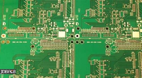
1.2 Panelization Considerations
- Breakaway Tabs and V-Scores: Facilitate easy separation of PCBs after assembly.
- Fiducial Marks: Aid in precise component placement during automated assembly.
1.3 Thermal Management
- Heat Dissipation: Incorporate thermal vias and heatsinks for high-power components.
- Copper Weight: Adjust copper thickness to manage current load and thermal performance.
2. Material Selection
2.1 PCB Substrate
- FR-4: Standard material for most applications, offering good mechanical and electrical properties.
- High-Frequency Materials: Required for RF and microwave applications (e.g., Rogers, PTFE).
- Flex and Rigid-Flex PCBs: Used in space-constrained or dynamic applications.
2.2 Solder Paste and Flux
- Lead-Free vs. Leaded Solder: Lead-free (e.g., SAC305) is RoHS-compliant but requires higher soldering temperatures.
- No-Clean vs. Water-Soluble Flux: No-clean flux reduces post-soldering cleaning requirements.
2.3 Component Quality
- Authentic and Traceable Components: Avoid counterfeit parts by sourcing from authorized suppliers.
- Moisture Sensitivity Level (MSL): Store moisture-sensitive components (e.g., BGAs, QFNs) properly to prevent popcorning during reflow.

3. Soldering Techniques
3.1 Reflow Soldering
- Temperature Profile: Optimize preheat, soak, reflow, and cooling phases to prevent defects like tombstoning or cold joints.
- Nitrogen Atmosphere: Reduces oxidation for high-quality solder joints.
3.2 Wave Soldering (for Through-Hole Components)
- Solder Wave Height and Speed: Adjust to ensure proper hole fill without bridging.
- Selective Soldering: Used for mixed-technology boards with both SMD and through-hole components.
3.3 Hand Soldering and Rework
- Temperature Control: Avoid overheating sensitive components.
- ESD Protection: Use grounded workstations to prevent electrostatic discharge damage.
4. Inspection and Testing
4.1 Automated Optical Inspection (AOI)
- Detects missing components, misalignment, and solder defects.
4.2 X-Ray Inspection (for BGAs and Hidden Joints)
- Identifies voids, cracks, and insufficient solder in concealed connections.
4.3 In-Circuit Testing (ICT) and Functional Testing
- Ensures electrical functionality and detects manufacturing defects.

5. Environmental and Process Controls
5.1 Cleanliness and Contamination Prevention
- No-Clean Processes: Minimize residue, but critical applications may still require cleaning.
- Ionic Contamination Testing: Ensures PCB cleanliness, especially for high-reliability applications.
5.2 Humidity and Temperature Control
- Storage Conditions: Maintain low humidity for moisture-sensitive components.
- Workshop Environment: Control temperature and humidity to prevent solder paste degradation.
5.3 ESD Protection
- ESD-Safe Workstations: Prevent damage to sensitive components.
- Proper Grounding: Ensures static charges are safely dissipated.
6. Quality Assurance and Documentation
6.1 Process Documentation
- Work Instructions (WIs): Standardize assembly procedures.
- Traceability Records: Track materials, components, and process parameters.
6.2 Failure Analysis and Continuous Improvement
- Root Cause Analysis (RCA): Investigate defects to prevent recurrence.
- Statistical Process Control (SPC): Monitor and optimize manufacturing processes.

Conclusion
PCBA processing involves numerous critical steps, each requiring careful attention to detail. By focusing on DFM, material selection, soldering techniques, inspection methods, and environmental controls, manufacturers can enhance product quality, reduce defects, and improve reliability. Implementing robust quality assurance practices further ensures consistency and traceability, leading to successful electronic product manufacturing.
By adhering to these best practices, PCBA manufacturers can achieve high yields, reduce costs, and deliver superior electronic assemblies to their customers.


