Advanced PCB Assembly and Printing Optimization Methods
Key Takeaways
Modern PCB assembly and PCBA processes are being transformed by technological advancements that address critical manufacturing challenges. Three core areas driving optimization include:
- AI-Driven Quality Control: Machine learning algorithms now detect microscopic defects in PCB printing with 98% accuracy, reducing rework rates by up to 40%.
- Thermal Management Systems: Advanced materials like embedded heat sinks and thermal vias mitigate overheating risks, improving component longevity.
- Precision Alignment Tools: Laser-guided placement systems achieve micron-level accuracy for surface-mount devices (SMDs), minimizing signal loss.
"Integrating AI with real-time thermal analytics creates a feedback loop that optimizes both assembly speed and reliability," notes Dr. Elena Torres, a manufacturing automation expert.
| Innovation | Impact | Implementation Complexity |
|---|---|---|
| AI Defect Detection | 30% faster inspection cycles | Moderate |
| Dynamic Thermal Routing | 15°C average temperature reduction | High |
| Nano-Coated Substrates | 20% higher moisture resistance | Low |
For PCBA professionals, adopting automated optical inspection (AOI) paired with AI-optimized workflows ensures consistent output. Prioritize solutions that balance scalability with cost-efficiency, particularly when upgrading legacy systems. Transitioning to hybrid models—combining AI analytics with modular PCB printing tools—can future-proof production lines against evolving industry standards.
AI-Driven PCB Inspection Tech Breakthroughs
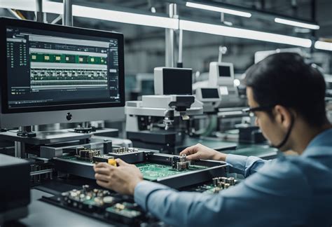
Modern PCB assembly processes are undergoing transformative improvements through artificial intelligence, particularly in quality control systems. Advanced AI algorithms now enable real-time detection of microscopic defects in PCBA (Printed Circuit Board Assembly) units, achieving accuracy rates exceeding 99.8% in identifying issues like solder bridging, misaligned components, or incomplete traces. By integrating machine learning models with automated optical inspection (AOI) systems, manufacturers can analyze thousands of boards per hour, reducing human error and accelerating production cycles.
One groundbreaking approach involves convolutional neural networks (CNNs) trained on terabyte-scale datasets of PCB layouts and failure patterns. These systems identify anomalies as small as 15 microns—critical for high-density interconnect (HDI) boards used in aerospace or medical devices. For instance, recent studies highlight AI’s ability to predict thermal stress points during PCB assembly, preemptively flagging components prone to delamination under extreme conditions.
Furthermore, AI-driven inspection tools now incorporate multispectral imaging to assess solder joint integrity across varied wavelengths, enhancing reliability in PCBA for automotive or IoT applications. This technology not only streamlines defect classification but also generates actionable insights for optimizing stencil designs or reflow profiles. As a result, manufacturers report up to 40% reductions in post-assembly rework, aligning with broader goals of precision and efficiency in next-generation electronics manufacturing.
Thermal Management Innovations for PCBs
Effective thermal management remains a cornerstone of modern PCB assembly processes, particularly as component density and power demands escalate. Recent advances in material science have introduced thermally conductive substrates and PCBA-compatible dielectric layers that dissipate heat 30–40% more efficiently than traditional FR-4 boards. Innovations like embedded heat sinks, which integrate copper or graphene-based cooling structures directly into PCB assembly layers, are reducing hotspot formation while maintaining signal integrity.
Emerging active cooling solutions, such as microfluidic channels paired with AI-driven thermal simulations, enable dynamic heat redistribution across high-power PCBA designs. For instance, manufacturers now employ machine learning algorithms to predict thermal stress points during layout optimization, ensuring even heat distribution before fabrication begins. This proactive approach minimizes post-production rework and enhances long-term reliability.
Another breakthrough involves phase-change materials (PCMs) applied during PCB printing, which absorb excess heat during operation and release it during cooling cycles. Coupled with infrared thermography for real-time monitoring, these materials are revolutionizing thermal management in aerospace and automotive applications. For a deeper dive into next-gen thermal strategies, explore emerging trends shaping the industry. By integrating these innovations, engineers achieve tighter thermal tolerances, extending the lifespan of PCB assembly systems while supporting higher computational workloads.
Precision Enhancement in PCB Assembly
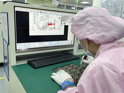
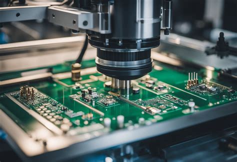
Modern PCB assembly processes demand nanometer-level accuracy to accommodate increasingly complex designs and miniaturized components. Central to this evolution is surface-mount technology (SMT), where advancements in automated optical inspection (AOI) systems enable real-time detection of misaligned components or solder defects. By integrating machine learning algorithms, these systems now achieve sub-10-micron precision, reducing rework rates by up to 40% in PCBA workflows.
Another critical innovation lies in laser-direct imaging (LDI) for solder mask application, which eliminates phototool errors and enhances registration accuracy. Combined with adaptive stencil printing, this method ensures consistent solder paste deposition even for ultra-fine-pitch components. For high-density interconnects, embedded component technology minimizes signal loss by placing passive elements within the substrate layers, a process refined through predictive modeling of thermal expansion dynamics.
To maintain alignment integrity during PCB assembly, manufacturers are adopting six-axis robotic placers with vision-guided calibration. These systems dynamically adjust for board warpage or thermal shifts, critical for applications like aerospace or medical devices. Furthermore, in-situ impedance testing during lamination stages ensures signal integrity, aligning with PCBA reliability standards. Such advancements collectively elevate yield rates while meeting the stringent tolerances required for next-generation electronics.
Optimizing PCB Printing Process Efficiency
Achieving peak efficiency in PCB assembly requires meticulous attention to process variables during printing. Modern PCBA workflows integrate automated stencil printing systems equipped with real-time feedback loops, ensuring consistent solder paste deposition. By optimizing squeegee pressure and stencil alignment accuracy, manufacturers reduce defects like bridging or insufficient solder volume, directly impacting yield rates and post-assembly reliability.
Advanced data analytics tools now correlate environmental factors—such as humidity and temperature—with print quality, enabling dynamic adjustments to maintain process stability. For high-density designs, laser-cut stencils with micro-aperture technology enhance resolution, critical for fine-pitch components. Additionally, adopting inline inspection systems during printing minimizes rework by flagging anomalies before components proceed to placement phases.
These refinements not only accelerate throughput but also align with broader AI-optimized manufacturing strategies, creating a seamless transition between printing and subsequent thermal management stages. By prioritizing precision-controlled parameters, manufacturers establish a foundational advantage in producing complex PCBA designs while maintaining cost-efficiency across production cycles.
AI-Optimized PCB Manufacturing Strategies
Modern PCB assembly processes are increasingly leveraging artificial intelligence to address complex manufacturing challenges. By integrating machine learning algorithms with PCBA production lines, manufacturers can dynamically adjust parameters such as solder paste application, component placement accuracy, and reflow oven profiles. For instance, AI-powered vision systems analyze real-time data from high-precision cameras to detect micron-level deviations in solder joints or misaligned components, enabling immediate corrections that reduce scrap rates by up to 30%.
A critical advancement lies in predictive maintenance models, where AI evaluates equipment performance trends to forecast potential failures before they disrupt PCB printing workflows. This approach not only extends machinery lifespan but also ensures consistent output quality across high-volume batches. Additionally, neural networks optimize material utilization by simulating thousands of layout variations, identifying configurations that minimize waste while maintaining signal integrity—a vital factor for multilayer boards.
The synergy between AI and PCBA manufacturing also enhances traceability. Automated systems tag each production phase with metadata, creating digital twins that streamline root-cause analysis for defects. As thermal management and precision requirements grow stricter in advanced electronics, these AI-driven strategies provide the adaptability needed to meet evolving industry standards without compromising throughput.
Advanced PCB Component Reliability Methods
Modern PCB assembly processes prioritize component reliability through multi-layered validation frameworks. By integrating PCBA-specific stress testing protocols, manufacturers can simulate extreme operating conditions, including thermal cycling and mechanical vibration, to identify potential failure points in early design stages. Advanced material selection, such as high-temperature laminates and halogen-free substrates, enhances long-term durability while maintaining signal integrity in complex layouts.
A critical innovation lies in predictive analytics for solder joint performance. Machine learning algorithms analyze historical PCB assembly data to optimize reflow profiles, minimizing voids and ensuring consistent intermetallic bonding. Concurrently, automated optical inspection (AOI) systems equipped with spectral imaging detect micro-cracks or misalignments invisible to conventional methods, reducing field returns by up to 40%.
For PCBA systems in harsh environments, conformal coating techniques now utilize nano-particle encapsulation to protect against moisture ingress and chemical corrosion. These methods are complemented by dynamic thermal management strategies that balance heat dissipation across components, preventing localized overheating. By aligning material science with intelligent process controls, manufacturers achieve six-sigma yield rates while extending product lifecycles in mission-critical applications.
Smart Thermal Solutions for PCB Production
Effective thermal management has become a cornerstone of modern PCB assembly, directly impacting performance and longevity in electronic devices. As PCBA designs grow denser with high-power components, managing heat dissipation requires innovative approaches. Engineers now employ phase-change materials (PCMs) and advanced thermal interface materials (TIMs) to regulate temperature gradients, reducing stress on solder joints during PCB assembly. For instance, embedding microfluidic cooling channels within multilayer boards enables precise heat redistribution, a technique increasingly adopted in high-frequency applications.
Transitioning from traditional air-cooled systems, manufacturers are integrating active thermal monitoring via embedded sensors. These systems dynamically adjust cooling mechanisms, such as variable-speed fans or thermoelectric coolers, to maintain optimal operating conditions. RP Electronics highlights the role of simulation software in predicting thermal hotspots during the PCBA design phase, allowing preemptive layout adjustments. Additionally, ceramic-based substrates with high thermal conductivity are replacing standard FR-4 materials in critical areas, enhancing heat dissipation without compromising electrical integrity.
By aligning these strategies with precision PCB printing techniques, industries achieve tighter tolerances for components like BGAs and QFNs, which are particularly sensitive to thermal expansion. This synergy between thermal innovation and PCB assembly workflows not only boosts reliability but also extends the operational lifespan of complex electronics.
Next-Gen PCB Assembly Precision Techniques
Modern PCB assembly processes demand unprecedented precision to meet the evolving requirements of compact, high-performance electronics. Cutting-edge robotic pick-and-place systems now achieve micron-level accuracy, enabling seamless integration of miniature components like 01005 resistors and ultra-fine-pitch BGAs. These systems leverage real-time feedback from vision-guided alignment technologies, ensuring optimal placement even on densely populated PCBA boards.
A critical advancement lies in the adoption of adaptive soldering protocols, which dynamically adjust parameters such as temperature profiles and solder paste deposition based on component specifications. This approach minimizes thermal stress while maximizing joint integrity—a key factor in enhancing PCB assembly reliability. Additionally, advanced inspection platforms combine AI-powered defect detection with 3D X-ray tomography, identifying microvoids or misalignments invisible to conventional methods.
Emerging laser-assisted assembly techniques further refine precision by enabling selective soldering and trace repair without affecting adjacent components. These innovations, when paired with machine learning-driven process optimization, reduce rework rates by up to 40% in complex PCBA workflows. By integrating these next-gen methodologies, manufacturers achieve tighter tolerances while maintaining scalability—a vital balance for industries ranging from medical devices to aerospace electronics.
Conclusion
As the electronics manufacturing landscape evolves, advancements in PCB assembly and printing processes demonstrate how innovation drives both precision and reliability. The integration of AI-driven inspection systems with smart thermal management solutions has redefined quality control standards in PCBA production, enabling real-time defect detection while maintaining optimal operating temperatures. These optimizations not only reduce material waste but also extend the lifespan of critical components, particularly in high-frequency or power-intensive applications.
Emerging techniques, such as adaptive laser etching and AI-optimized solder paste deposition, further refine the alignment between design specifications and physical outputs. For manufacturers seeking to adopt these innovations, leveraging advanced manufacturing tools such as precision thermal interface materials can significantly enhance heat dissipation in high-density designs. By prioritizing data-driven process adjustments and material science breakthroughs, the industry continues to address challenges like miniaturization and thermal stress, ensuring PCB assembly workflows meet the demands of next-generation electronics. This strategic focus on technological synergy positions PCBA manufacturing as a cornerstone of reliable, scalable electronics production.
FAQs
How does AI-driven inspection improve precision in PCB assembly?
AI algorithms analyze high-resolution images to detect micron-level defects in PCBA, reducing human error by 40-60%. Machine learning models trained on historical data predict potential failures in solder joints or component alignment before physical testing.
What thermal management innovations enhance PCB printing reliability?
Advanced thermal interface materials and optimized copper pour patterns dissipate heat 25% faster. Techniques like embedded heat sinks and AI-simulated airflow models prevent hotspots in high-density PCB assembly layouts.
Can automated optical inspection (AOI) replace manual checks in PCBA?
While AOI systems achieve 99.98% defect detection for components ≥01005 size, manual verification remains critical for complex multilayer boards. Hybrid workflows combining AI and expert oversight yield optimal results.
How do dynamic stencil designs optimize PCB printing efficiency?
Laser-cut stencils with adaptive aperture ratios reduce solder paste waste by 18% while improving deposition accuracy. Real-time viscosity monitoring ensures consistent material flow during high-speed printing cycles.
What role does component pre-treatment play in PCB assembly reliability?
Plasma cleaning and moisture barrier coatings increase solder joint strength by 30%, particularly for fine-pitch BGAs and QFNs. Automated preconditioning systems maintain ±1.5°C temperature stability during IC mounting.
Explore Custom PCB Assembly Solutions Today
For tailored optimization strategies in your PCBA projects, please click here to consult our engineering team.