PCB Baking Stacking Methods and Key Considerations
Introduction
Printed Circuit Board (PCB) baking is a critical process in electronics manufacturing, especially for moisture-sensitive devices. Proper baking ensures that moisture absorbed by the PCB is removed, preventing defects such as delamination, blistering, or “popcorning” during reflow soldering. The effectiveness of PCB baking depends on several factors, including the stacking method, temperature, duration, and handling procedures. This article explores different PCB baking stacking methods and outlines essential considerations to ensure optimal results.
Why is PCB Baking Necessary?
PCBs, particularly those made with hygroscopic materials like FR-4, can absorb moisture from the environment. When exposed to high temperatures during soldering, trapped moisture vaporizes rapidly, leading to internal pressure buildup. This can cause:
- Delamination – Separation of PCB layers
- Blistering – Surface defects due to gas expansion
- Voiding – Poor solder joint formation
- Component Damage – Cracking or failure of moisture-sensitive parts
To mitigate these risks, PCBs are baked before assembly to remove excess moisture.
PCB Baking Stacking Methods
The way PCBs are stacked during baking significantly impacts heat distribution and moisture removal. Improper stacking can lead to uneven drying, warping, or contamination. Below are common PCB baking stacking methods:
1. Horizontal Stacking (Flat Baking)
- PCBs are laid flat on baking trays with sufficient spacing (typically 10-20 mm) between them.
- Advantages:
- Minimizes warping due to even heat exposure.
- Suitable for thin or flexible PCBs.
- Disadvantages:
- Requires more oven space.
- Slower moisture removal if airflow is restricted.
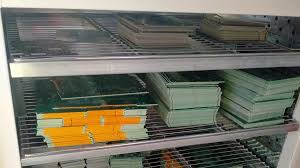
2. Vertical Stacking (Rack Baking)
- PCBs are placed vertically in slots or racks, allowing air circulation between boards.
- Advantages:
- Efficient use of oven space.
- Better airflow for faster drying.
- Disadvantages:
- Risk of warping if boards are too thin.
- Requires stable racks to prevent toppling.
3. Spacer-Based Stacking
- Small spacers (non-conductive) are placed between PCBs to maintain gaps.
- Advantages:
- Prevents direct contact between boards, reducing contamination.
- Allows controlled airflow.
- Disadvantages:
- Manual placement increases handling time.
- Spacers must be heat-resistant.
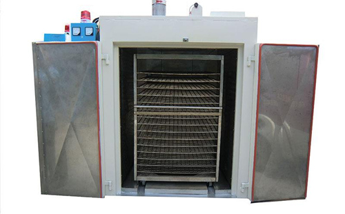
4. Conveyorized Baking (Continuous Baking)
- Used in high-volume production where PCBs move through a conveyorized oven.
- Advantages:
- Consistent baking conditions.
- High throughput.
- Disadvantages:
- Requires precise temperature control.
- Not suitable for small batches.
Key Considerations for PCB Baking
To ensure effective moisture removal without damaging PCBs, the following factors must be carefully controlled:
1. Temperature Settings
- Typical Range: 105°C to 125°C (IPC standards recommend 125°C for most PCBs).
- Avoid Excessive Heat: Temperatures above 150°C can damage laminate materials.
- Preheat Gradually: Sudden temperature spikes can cause thermal stress.
2. Baking Duration
- Standard Baking Time: 2 to 12 hours, depending on PCB thickness and moisture sensitivity level (MSL).
- Thicker PCBs (>2mm): Require longer baking (up to 24 hours).
- Moisture-Sensitive Devices (MSD): Follow IPC/JEDEC J-STD-033 guidelines.
3. Humidity Control
- Bake PCBs in a low-humidity environment (<5% RH preferred).
- Use nitrogen-purged ovens for highly sensitive PCBs.
4. Handling After Baking
- Cooling: Allow PCBs to cool gradually to avoid thermal shock.
- Storage: Store baked PCBs in moisture barrier bags (MBBs) with desiccants if not used immediately.
- Time Constraints: Assemble within 24-48 hours after baking (depending on MSL).
5. Avoiding Contamination
- Use clean, static-free baking trays.
- Do not stack PCBs directly on top of each other without spacers.
- Ensure oven interior is free from dust and residues.
6. Monitoring and Documentation
- Use data loggers to track temperature and humidity during baking.
- Record baking time, temperature, and batch details for traceability.
Common Mistakes in PCB Baking
- Overstacking: Too many PCBs in a single batch can block airflow, leading to uneven drying.
- Insufficient Baking Time: Removing PCBs too early leaves residual moisture.
- Improper Cooling: Rapid cooling can introduce new moisture or cause warping.
- Ignoring MSL Classifications: Different components require specific baking conditions.
Conclusion
Proper PCB baking is essential for ensuring reliability in electronic assemblies. The stacking method (horizontal, vertical, or spacer-based) must be chosen based on PCB type, oven capacity, and production volume. Critical parameters such as temperature, duration, and humidity must be strictly controlled to prevent moisture-related defects. By following industry standards (IPC/JEDEC) and implementing best practices, manufacturers can enhance PCB quality and reduce rework costs.
For high-reliability applications, continuous monitoring and proper handling after baking are just as crucial as the baking process itself. Investing in automated baking systems with precise environmental controls can further improve consistency and yield in PCB manufacturing.