Optimizing PCB Layout:Strategic Placement of Passive Components Around PMICs
Introduction
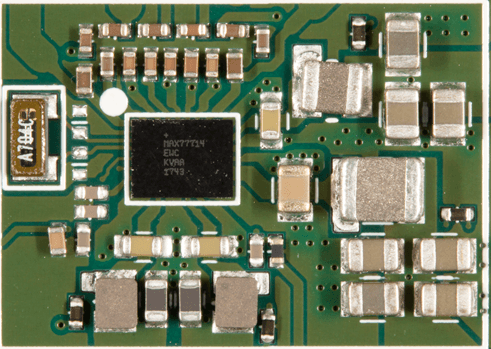
Power Management Integrated Circuits (PMICs) are essential components in modern electronic devices, responsible for regulating and distributing power to various subsystems. The performance of a PMIC is heavily influenced by the placement of its surrounding passive components—capacitors, resistors, and inductors. Proper PCB layout around PMICs can significantly impact power efficiency, thermal performance, electromagnetic interference (EMI), and overall system reliability. This 2000-word article provides comprehensive guidelines for optimizing passive component placement around PMICs to achieve optimal PCB performance.
Understanding PMIC Requirements
Power Delivery Network Fundamentals
The power delivery network (PDN) surrounding a PMIC consists of:
- Input capacitors for bulk energy storage and high-frequency filtering
- Output capacitors for voltage regulation and transient response
- Feedback network resistors for voltage setting and regulation
- Bootstrap capacitors for gate drivers (when applicable)
- Inductors for switching regulator circuits
Each component plays a critical role in the PMIC’s operation, and their placement affects:
- Power integrity
- Signal integrity
- Thermal management
- EMI/EMC performance
PMIC-Specific Considerations
Before laying out components, review:
- The PMIC datasheet for manufacturer-recommended layouts
- Current requirements for each power rail
- Switching frequencies of DC-DC converters
- Thermal characteristics and expected power dissipation
- Board space constraints and layer stackup
Key Principles for Passive Component Placement
1. Input Capacitor Placement
Priority: Highest – These capacitors handle large current transients
Placement Guidelines:
- Place bulk capacitors (typically electrolytic or tantalum) closest to the power input connector
- Position ceramic decoupling capacitors as close as possible to the PMIC’s input pins
- Use multiple vias for low-impedance connections to power planes
- For multi-phase regulators, ensure balanced capacitor placement
Optimal Configuration:
[Power Input] → [Bulk Cap (10-100μF)] → [Mid-range Cap (1-10μF)] → [Ceramic Decoupling Cap (0.1-1μF @ PMIC pin)]
2. Output Capacitor Placement
Priority: High – Affects regulator stability and transient response
Placement Guidelines:
- Place output capacitors closest to the PMIC’s output pins
- For switching regulators, position capacitors to form a tight loop with the inductor and IC
- Use small-footprint capacitors (0402 or smaller) for highest-frequency decoupling
- Distribute capacitors around all output pins for multi-output PMICs
Critical Note: The first ceramic capacitor after the inductor should be within 2-3mm of the switching node.
3. Inductor Placement (for Switching Regulators)
Priority: Medium-High – Affects EMI and efficiency
Placement Guidelines:
- Position inductors as close as possible to the PMIC’s SW pins
- Orient inductors to minimize loop area with input/output capacitors
- Avoid placing sensitive signals near inductor magnetic fields
- Use shielded inductors in noise-sensitive applications
Thermal Consideration: Ensure adequate spacing between inductors and heat-generating components.
4. Feedback Network Placement
Priority: Medium – Critical for regulation accuracy
Placement Guidelines:
- Place feedback resistors and compensation components close to the FB pin
- Route feedback traces away from noisy switching nodes
- Use a ground plane under feedback components for stability
- Keep feedback traces short and direct
Pro Tip: Implement a Kelvin connection for high-current outputs by sensing voltage directly at the load.
5. Bootstrap Capacitor Placement
Priority: Medium (for switching regulators)
Placement Guidelines:
- Place bootstrap capacitors adjacent to their respective BOOT pins
- Minimize loop area between BOOT, SW, and BST capacitors
- Use capacitors with low ESR and appropriate voltage ratings
Layer Stackup Considerations
An optimal layer stackup enhances PMIC performance:
- Top Layer: PMIC, critical passives, and high-frequency routing
- Inner Layer 1: Solid ground plane (critical for return paths)
- Inner Layer 2: Power planes (split appropriately)
- Bottom Layer: Less critical passives and lower-speed signals
Key Practices:
- Use multiple vias for component connections to reduce impedance
- Implement via-in-pad technology for space-constrained designs
- Ensure continuous ground planes beneath switching circuits
Thermal Management Through Component Placement
Proper passive component placement aids thermal performance:
- Heat Distribution:
- Position components to avoid hot spots
- Use ground planes as heat spreaders
- Place thermal vias under PMIC thermal pads
- Airflow Considerations:
- Orient tall components (like electrolytic caps) to not block airflow
- Distribute heat-generating components across the board
- Thermal Relief:
- Balance heat dissipation with electrical performance
- Use appropriate copper weights for high-current paths
EMI Reduction Techniques
Strategic passive component placement reduces EMI:
- Loop Area Minimization:
- Keep high di/dt loops as small as possible
- Place input capacitors, PMIC, and inductor in tight formation
- Shielding Strategies:
- Use grounded copper as shields between noisy and sensitive areas
- Position capacitors to act as high-frequency shields
- Component Orientation:
- Align capacitors to cancel magnetic fields
- Orient inductors at 90° to each other when multiple are present
High-Current Layout Techniques
For PMICs handling high currents (>3A):
- Use Wide Traces:
- Follow IPC-2152 standards for current capacity
- Implement copper pours for power paths
- Current Sensing:
- Place sense resistors close to the PMIC
- Route sense lines differentially when possible
- Via Strategies:
- Use multiple vias in parallel for current sharing
- Place vias close to component pads
Advanced Placement Techniques
1. Component Embedding
For space-constrained designs:
- Consider embedding passive components in inner layers
- Use 0201 or smaller components when necessary
2. 3D Placement Optimization
Evaluate component placement in three dimensions:
- Height restrictions for assembly
- Component shadowing effects
- Wave soldering considerations
3. Manufacturing Considerations
Design for manufacturability:
- Maintain proper component spacing for pick-and-place machines
- Follow solder mask and silkscreen guidelines
- Consider reflow soldering thermal profiles
Verification and Testing
After placement, verify through:
- Electrical Testing:
- Measure power integrity with oscilloscope
- Check for excessive ripple and noise
- Thermal Imaging:
- Identify hot spots under load
- Verify component thermal performance
- EMI Scanning:
- Conduct near-field scans
- Identify EMI radiation sources
Common Mistakes to Avoid
- Inadequate Decoupling:
- Using too few or improperly placed decoupling capacitors
- Neglecting high-frequency decoupling needs
- Poor Grounding:
- Creating ground loops
- Insufficient ground connections
- Thermal Issues:
- Overlooking thermal relief requirements
- Ignoring component power dissipation ratings
- Manufacturing Oversights:
- Placing components too close for assembly
- Ignating solder mask requirements
Case Study: Optimal PMIC Layout Example
Scenario: 5V to 1.2V buck converter @ 2A
Optimal Placement:
- Input capacitors:
- 10μF X7R (0805) within 2mm of VIN pin
- 1μF X7R (0603) adjacent to PMIC
- 0.1μF X7R (0402) closest to pin
- Output capacitors:
- 22μF X5R (0805) near inductor
- 4.7μF X7R (0603) near output pin
- 1μF X7R (0402) closest to output
- Inductor:
- Shielded 2.2μH within 3mm of SW pin
- Oriented to minimize loop area
- Feedback:
- 1kΩ/2kΩ divider (0402) within 3mm of FB pin
- Grounded directly to PMIC ground pad
Results: Achieved <30mV output ripple and 92% efficiency at full load.

Conclusion
Optimizing passive component placement around PMICs requires careful consideration of electrical, thermal, and mechanical factors. By following the guidelines presented—prioritizing input capacitor placement, minimizing loop areas, implementing proper grounding strategies, and considering thermal management—designers can significantly improve power delivery network performance. Always refer to the specific PMIC’s datasheet for manufacturer-recommended layouts and validate designs through thorough testing. Proper PCB layout practices for PMIC surrounding components ultimately lead to more reliable, efficient, and higher-performance electronic systems.
Remember that each design presents unique challenges, and these guidelines should be adapted to specific application requirements, balancing often-competing priorities of performance, size, cost, and manufacturability.