What to Draw on Each Layer of a PCB: A Comprehensive Guide
Printed Circuit Boards (PCBs) are the backbone of modern electronics, providing mechanical support and electrical connections between components. A well-designed PCB ensures optimal performance, signal integrity, and manufacturability. To achieve this, designers must understand the purpose of each PCB layer and what should be drawn on them.
This article explores the different layers in a PCB and their respective functions, helping engineers and hobbyists create efficient and reliable circuit boards.
1. Introduction to PCB Layers
PCBs can be single-layer, double-layer, or multi-layer, depending on the complexity of the circuit. Each layer serves a specific purpose:
- Signal Layers: Carry electrical signals between components.
- Power & Ground Planes: Provide stable voltage distribution and reduce noise.
- Mechanical Layers: Define the board’s physical structure.
- Silkscreen Layers: Display component labels and reference designators.
- Solder Mask Layers: Protect copper traces from oxidation and prevent solder bridges.
- Paste & Drill Layers: Assist in assembly and fabrication.
Let’s examine each layer in detail.
2. Signal Layers (Top, Bottom, and Internal Layers)
Signal layers contain conductive copper traces that connect components. The number of signal layers depends on the PCB’s complexity.
A. Top Layer (Component Layer)
- What to Draw:
- Component footprints (pads, vias, and traces).
- High-speed signal traces (preferably shorter paths).
- Critical signal routes that require minimal interference.
- Considerations:
- Avoid running sensitive signals near noisy components (e.g., power regulators).
- Use wider traces for high-current paths.
B. Bottom Layer (Solder Layer)
- What to Draw:
- Additional signal traces that couldn’t fit on the top layer.
- Ground return paths for better signal integrity.
- Low-frequency signals (less susceptible to noise).
- Considerations:
- Minimize via transitions between layers to reduce impedance discontinuities.
C. Internal Signal Layers (In Multilayer PCBs)
- What to Draw:
- High-speed differential pairs (e.g., USB, HDMI).
- Controlled impedance traces (requires precise calculations).
- Sensitive analog signals (shielded from digital noise).
- Considerations:
- Use ground planes adjacent to signal layers for EMI reduction.
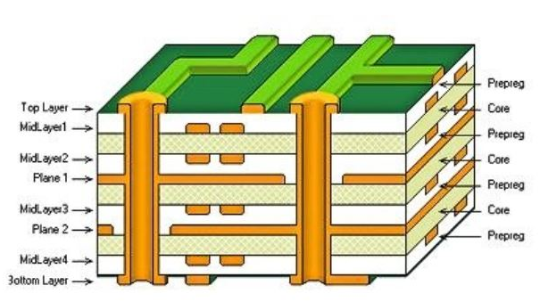
3. Power and Ground Planes
Power and ground planes ensure stable voltage distribution and reduce electromagnetic interference (EMI).
A. Power Plane
- What to Draw:
- A solid copper pour connected to the power supply (e.g., VCC, 3.3V, 5V).
- Split planes for multiple voltage levels (e.g., separate 3.3V and 5V regions).
- Considerations:
- Avoid sharp corners to prevent high current density.
- Use decoupling capacitors near ICs to minimize voltage drops.
B. Ground Plane
- What to Draw:
- A continuous copper area connected to GND.
- Return paths for high-frequency signals.
- Considerations:
- Ensure low impedance by minimizing splits.
- Use stitching vias to connect ground planes in multilayer PCBs.
4. Mechanical Layers (Board Outline & Keep-Out
Mechanical layers define the PCB’s physical dimensions and restrictions.
A. Board Outline Layer
- What to Draw:
- The exact shape and size of the PCB.
- Cutouts, slots, and mounting holes.
- Considerations:
- Follow manufacturer tolerances for dimensions.
B. Keep-Out Layer
- What to Draw:
- Restricted areas where no copper or components should be placed.
- Clearance zones near high-voltage components.
- Considerations:
- Ensure compliance with safety standards (e.g., creepage and clearance for high voltage).
5. Silkscreen Layers (Top & Bottom Overlay)
Silkscreen layers provide visual guidance for assembly and debugging.
A. Top Silkscreen
- What to Draw:
- Component reference designators (e.g., R1, C2, U3).
- Polarity indicators (e.g., “+” for capacitors, pin 1 markers for ICs).
- Company logos, version numbers, and labels.
- Considerations:
- Avoid placing text over pads or vias.
B. Bottom Silkscreen
- What to Draw:
- Additional labels if space permits.
- Assembly instructions (e.g., “Place this side down”).
6. Solder Mask Layers (Top & Bottom)
Solder mask is a protective coating that prevents short circuits and oxidation.
A. Top Solder Mask
- What to Draw:
- Openings for exposed pads (e.g., SMD components, test points).
- Custom shapes for heat dissipation (e.g., thermal pads).
- Considerations:
- Ensure proper mask expansion around pads.
B. Bottom Solder Mask
- What to Draw:
- Similar to the top layer, but for bottom-side components.
7. Solder Paste Layers (Top & Bottom Paste)
These layers define where solder paste is applied in Surface-Mount Technology (SMT) assembly.
A. Top Paste
- What to Draw:
- Stencil openings for SMD pads.
- Considerations:
- Adjust aperture sizes for fine-pitch components.
B. Bottom Paste
- What to Draw:
- Paste for bottom-side SMD components (if applicable).
8. Drill Layers (Holes & Vias)
Drill layers specify hole locations for through-hole components and vias.
A. Drill Drawing Layer
- What to Draw:
- Symbols representing hole sizes and positions.
- Considerations:
- Differentiate between plated and non-plated holes.
B. NC Drill Layer (Gerber)
- What to Draw:
- Machine-readable drill data (coordinates and sizes).
9. Additional Layers (Special Cases)
Some PCBs require extra layers for specific purposes:
- Impedance Control Layers: For high-frequency designs.
- Flex Layers: In flexible PCBs, defining bend areas.
- Carbon Ink Layers: For touch-sensitive buttons.
10. Best Practices for PCB Layer Management
- Prioritize Signal Integrity: Route critical traces first.
- Minimize Crosstalk: Separate high-speed and analog signals.
- Optimize Power Distribution: Use solid planes for power and ground.
- Follow Design Rules: Adhere to manufacturer specifications.
- Verify with DRC (Design Rule Check): Ensure no errors before fabrication.
11. Conclusion
Understanding what to draw on each PCB layer is crucial for designing functional and manufacturable boards. Signal layers handle connections, power planes ensure stable voltage, mechanical layers define the board shape, and auxiliary layers (silkscreen, solder mask, paste, and drill) aid in assembly. By following best practices, designers can optimize performance, reduce EMI, and improve reliability.
Whether you’re designing a simple Arduino shield or a complex multilayer PCB, mastering layer usage will lead to better, more efficient designs.