Optimizing PCB Layout: Proper Placement of Passive Components Around PMICs
Introduction
Power Management Integrated Circuits (PMICs) are essential components in modern electronic devices, responsible for converting, regulating, and distributing power to various subsystems. While much attention is given to selecting the right PMIC for an application, the proper placement of passive components around these devices is equally critical for optimal performance. This 2000-word article explores best practices for placing passive components (capacitors, resistors, and inductors) around PMICs to achieve efficient power delivery, minimize noise, and ensure stable operation.
Understanding PMIC Requirements
Before diving into component placement, it’s crucial to understand the specific requirements of your PMIC:
- Input Voltage Requirements: Determines input capacitor selection and placement
- Output Voltage and Current Specifications: Affects output capacitor network design
- Switching Frequency: Influences capacitor and inductor characteristics
- Control Loop Stability Requirements: Impacts feedback network component placement
- Thermal Considerations: Affects overall component spacing and layout
Input Capacitor Placement
The input capacitors serve multiple critical functions:
- Provide local charge storage for high current demands
- Filter input voltage noise
- Reduce input voltage ripple
- Minimize high-frequency switching noise propagation back to the power source
Best Practices for Input Capacitor Placement:
- Proximity to PMIC Pins: Place input capacitors as close as possible to the PMIC’s VIN and GND pins. Ideally, the capacitor should be within 2-3mm of the device.
- Use Multiple Capacitor Values: Implement a combination of bulk capacitors (10-100µF) and smaller ceramic capacitors (0.1-10µF) to handle different frequency ranges.
- Minimize Loop Area: Arrange the input capacitor to minimize the loop area formed by the VIN trace, capacitor, and ground return path. This reduces parasitic inductance.
- Direct Connection to Ground Plane: Connect the capacitor’s ground terminal directly to the ground plane through a via adjacent to the pad, not through a long trace.
- High-Frequency Capacitors Closest: Place the smallest value (highest frequency) capacitors physically closest to the PMIC pins.
Output Capacitor Placement
Output capacitors are critical for:
- Maintaining stable output voltage during load transients
- Reducing output voltage ripple
- Compensating the control loop for stability
Best Practices for Output Capacitor Placement:
- Immediate Proximity to Output Pins: Position output capacitors as close as possible to the PMIC’s VOUT and GND pins, with the smallest capacitors nearest.
- Multiple Parallel Capacitors: Use a combination of ceramic and (if needed) electrolytic capacitors to handle both high-frequency and low-frequency components.
- Low-ESR Selection: Choose capacitors with low equivalent series resistance (ESR) to minimize voltage ripple and power loss.
- Proper Grounding: Ensure all output capacitor ground connections tie back to the same local ground point as the PMIC’s ground reference.
- Consider Load Location: If the load is some distance from the PMIC, consider adding additional bulk capacitance near the load.
Feedback Network Component Placement
The feedback network (typically resistors and sometimes capacitors) sets the output voltage and affects stability:
- Critical Signal Path: Treat the feedback path as a sensitive analog signal.
- Proximity to PMIC: Place feedback components close to the PMIC’s FB pin.
- Avoid Noisy Areas: Route feedback traces away from switching nodes and high-current paths.
- Kelvin Connection: When possible, connect the feedback network directly to the output capacitor pads rather than along the output trace.
- Ground Reference: Ensure the feedback divider’s ground reference connects to a clean, stable ground point.
Bootstrap and Compensation Components
Many PMICs require additional components for proper operation:
- Bootstrap Capacitors: For buck converters with high-side switches, place the bootstrap capacitor and diode very close to the appropriate pins.
- Compensation Networks: Place compensation components (RC networks) exactly as specified in the datasheet, typically adjacent to the COMP or similar pin.
- Soft-Start Capacitors: These timing capacitors should be placed near their respective pins with short traces.
Inductor Placement (for Switching Regulators)
For PMICs with integrated switching regulators, inductor placement is critical:
- Minimize Loop Area: Keep the switch node (connection between PMIC and inductor) as small as possible to reduce EMI.
- Orientation: Place the inductor to minimize coupling with sensitive circuits.
- Grounding: Ensure the output capacitor ground is close to the inductor’s ground connection.
- Thermal Considerations: Allow space for inductor heating and keep away from temperature-sensitive components.
General PCB Layout Guidelines
Beyond specific component placement, follow these general rules:
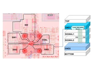
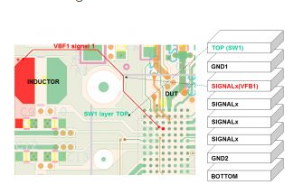
- Layer Stackup: Use at least a 4-layer board with dedicated power and ground planes when possible.
- Ground Plane: Maintain a solid ground plane beneath the PMIC and its associated components.
- Thermal Relief: Provide adequate thermal vias for heat dissipation from the PMIC and power components.
- Trace Width: Use appropriately wide traces for high-current paths (input, output, and switch nodes).
- Via Placement: Use multiple vias for high-current connections to reduce impedance and improve thermal performance.
- Component Orientation: Align components to simplify routing and minimize trace lengths.
Common Mistakes to Avoid
- Improper Grounding: Creating ground loops or separating analog and power grounds incorrectly.
- Long Traces on Critical Paths: Excessive trace length on switch nodes, feedback paths, or high-current routes.
- Insufficient Capacitance: Not providing enough or the right type of capacitance at both input and output.
- Ignoring Thermal Considerations: Not providing adequate copper area or vias for heat dissipation.
- Poor Component Sequencing: Placing components in an order that creates unnecessary trace lengths or loops.
Advanced Techniques
For demanding applications, consider these advanced techniques:
- Embedded Components: Use buried capacitance within the PCB stackup for additional high-frequency decoupling.
- 3D Component Placement: In complex designs, consider placing some capacitors on the opposite side of the board directly beneath the PMIC.
- Simulation: Use power integrity simulation tools to verify your layout before fabrication.
- Current Density Analysis: Verify that copper areas can handle expected currents without excessive voltage drop.
Case Study: Optimal PMIC Layout
Consider a typical buck converter PMIC implementation:
- Input Section:
- 10µF ceramic capacitor placed within 2mm of VIN pin
- 100µF bulk capacitor placed within 5mm
- All grounds connected directly to plane with multiple vias
- Switch Node:
- Inductor placed adjacent to PMIC with minimal trace length
- Switch node kept small and away from sensitive signals
- Output Section:
- 22µF ceramic capacitor placed within 1mm of VOUT
- Additional 100µF capacitor placed near load
- Feedback:
- Divider resistors placed within 3mm of FB pin
- Feedback trace routed away from switch node
- Ground reference taken from output capacitor ground
Conclusion
Proper placement of passive components around PMICs is both an art and a science that significantly impacts the performance, efficiency, and reliability of power delivery systems. By following these guidelines—focusing on minimizing loop areas, reducing parasitic elements, maintaining proper grounding, and considering thermal aspects—designers can create PCB layouts that fully realize the potential of their chosen PMICs. Always consult the specific PMIC’s datasheet for device-specific recommendations and verify designs through prototyping and testing when possible. Careful attention to passive component placement will result in cleaner power, better efficiency, and more stable operation across all load conditions.