Post-Processing in PCB Design: Essential Steps for Manufacturing and Reliability
Introduction
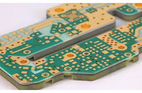
Printed Circuit Board (PCB) design is a complex process that involves schematic capture, component placement, routing, and verification. However, the work does not end once the layout is complete. Post-processing is a critical phase that ensures the design is manufacturable, reliable, and meets industry standards. This article explores the key post-processing steps in PCB design, including Design for Manufacturability (DFM) checks, Gerber file generation, solder mask and silkscreen adjustments, panelization, and final validation.
1. Design for Manufacturability (DFM) Checks
Before sending a PCB design for fabrication, engineers must perform Design for Manufacturability (DFM) checks to identify potential issues that could affect production yield or performance. Key DFM considerations include:
1.1 Trace Width and Spacing
- Ensure traces meet the manufacturer’s minimum width and spacing requirements.
- High-current traces must be wider to prevent overheating.
- High-speed signals may require controlled impedance routing.
1.2 Drill Hole and Via Validation
- Verify that via sizes are manufacturable (laser-drilled microvias vs. mechanical drills).
- Ensure annular rings are sufficient to prevent breakout during drilling.
1.3 Copper Balancing
- Uneven copper distribution can cause warping during reflow soldering.
- Use thieving (adding non-functional copper) to balance copper density.
1.4 Solder Mask and Silkscreen Clearance
- Ensure solder mask openings (pads) are correctly sized to prevent solder bridging.
- Silkscreen text should not overlap pads or vias.
1.5 Component Placement and Footprint Verification
- Confirm that component footprints match datasheet specifications.
- Check for sufficient spacing between components for assembly.
Many PCB design tools (e.g., Altium Designer, KiCad, Cadence Allegro) include automated DFM checkers to flag potential issues.
2. Gerber File Generation
Gerber files are the standard format used by PCB manufacturers to produce boards. Each layer (copper, solder mask, silkscreen, drill files) is exported separately.
2.1 Layer Stack-Up Configuration
- Define the correct layer order (signal, power, ground planes).
- Specify dielectric materials and thicknesses for impedance control.
2.2 Gerber File Types
- Copper Layers (GTL, GBL, Gx) – Top and bottom conductive layers.
- Solder Mask (GTS, GBS) – Openings for soldering.
- Silkscreen (GTO, GBO) – Component labels and logos.
- Drill Files (Excellon format) – Hole locations and sizes.
- IPC-356 Netlist – Used for testing continuity.
2.3 Verification with Gerber Viewers
Before submission, use a Gerber viewer (e.g., GC-Prevue, CAM350, KiCad GerbView) to confirm:
- No missing or misaligned layers.
- Correct pad shapes and drill holes.
3. Solder Mask and Silkscreen Adjustments
The solder mask and silkscreen layers improve PCB reliability and assembly accuracy.
3.1 Solder Mask Considerations
- Color Selection – Common options: green, blue, red, black.
- Clearance Around Pads – Typically 0.05–0.1mm larger than pads.
- Tented Vias – Covering vias with solder mask to prevent solder wicking.
3.2 Silkscreen Legibility
- Use readable fonts (≥0.8mm height).
- Avoid placing text under components.
- Include polarity markers, pin-1 indicators, and reference designators.
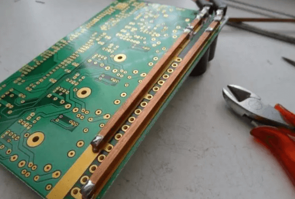
4. Panelization for Mass Production
For efficient manufacturing, multiple PCBs are often grouped into a single panel.
4.1 Panel Design Methods
- Tab Routing – Small tabs hold boards together; breakaway after assembly.
- V-Scoring – Partial cuts for easy separation.
- Mouse Bites – Small perforations for snapping apart.
4.2 Fiducial Marks and Tooling Holes
- Add fiducials (reference markers) for automated pick-and-place machines.
- Include tooling holes for alignment during fabrication.
5. Final Validation and Testing
Before releasing files to the manufacturer, perform final checks:
5.1 Electrical Rule Check (ERC) and Design Rule Check (DRC)
- Confirm no unconnected nets or short circuits.
- Verify power and ground integrity.
5.2 Signal Integrity (SI) and Power Integrity (PI) Analysis
- Simulate high-speed signal paths for reflections and crosstalk.
- Ensure stable power delivery with decoupling capacitors.
5.3 Thermal Analysis
- Identify hotspots that may require thermal vias or heatsinks.
5.4 Prototype Testing
- Order a small batch for functional testing before full production.
6. Documentation and Assembly Files
Provide complete documentation to the manufacturer and assembly house:
- Bill of Materials (BOM) – List of components with part numbers.
- Pick-and-Place File – Coordinates for automated assembly.
- Assembly Drawings – Mechanical dimensions and special instructions.
Conclusion
Post-processing is a crucial stage in PCB design that bridges the gap between a digital layout and a physical, functional board. By performing thorough DFM checks, generating accurate Gerber files, optimizing solder mask and silkscreen, panelizing efficiently, and validating the design through simulations and prototypes, engineers can ensure high-quality, manufacturable PCBs. Neglecting these steps can lead to costly rework, delays, or even complete board failures. A disciplined post-processing workflow enhances reliability, reduces production costs, and accelerates time-to-market for electronic products.