Skip to content
Andwin Circuits
  • Home
  • ProductsExpand
    • HDI multilayer PCB
    • Rigid Flex PCB
    • Flex pcb
    • Special PCBExpand
      • High Frequency PCBExpand
        • Rogers RO4350B PCB
        • Rogers RO4003 pcb
        • Rogers RO3003 PCB
        • Rogers 5880 PCB
        • DICLAD 527 PCB
        • Taconic TLX series
        • Taconic TLX-8 RF PCB
        • Taconic TLX-9 RF PCB
      • High speed pcbExpand
        • Megtron 6 High Speed PCB
        • TU-872 SLK Sp High Speed
      • High TG PCBExpand
        • SHENGYI SH260 PCB
        • ISOLA 370HR PCB
        • ISOLA IS410 PCB
        • ISOLA IS420 PCB
      • Heavy copper PCB
      • Copper coin pcb
      • Copper inlay PCB
    • Metal Core PCBExpand
      • Copper core pcb
      • Aluminum PCB
      • 2 Layers Aluminum PCB
      • Direct thermal MCPCB
      • 2 Layers Direct Thermal
    • Ceramic PCBExpand
      • DPC ceramic PCB
      • DBC ceramic PCB
      • Thick film Ceramic PCB
      • Al2O3 Alumina PCB
      • AIN ALN ceramic PCB
      • IGBT Ceramic PCB
  • ServiceExpand
    • PCB Assembly
    • Quick turn PCB assembly
    • PCBA conformal coating
  • IndustryExpand
    • Telecommunication
    • IoT and Wireless
    • Industrial Control
    • Thermal management
    • Power and Energy
    • IC test board
    • Automative
    • Medical
  • CapabilityExpand
    • Rigid PCB
    • Rigid flex PCB
    • Metal core PCB
    • PCB Assembly
  • TechnologyExpand
    • Blogs
    • Via in pad
    • PCB E-test
    • PCB stack up
    • MCPCB panelization
    • Controlled impedance PCB
  • AboutExpand
    • About us
    • Certification
    • Factory Tour
  • Contact
Andwin Circuits
Home / Blogs / WiFi Antenna Requirements for PCB Layout, Routing, and Mechanical Structure

WiFi Antenna Requirements for PCB Layout, Routing, and Mechanical Structure

ByGrace May 24, 2025July 7, 2025

1. Introduction

WiFi antennas are critical components in wireless communication systems, directly impacting signal quality, range, and data throughput. Proper integration of WiFi antennas into Printed Circuit Board (PCB) designs requires careful consideration of layout, routing, and mechanical structure to minimize interference, optimize radiation patterns, and ensure reliable wireless performance. This paper explores the key requirements for WiFi antenna placement, PCB routing techniques, and structural considerations to achieve optimal RF performance.

Contact us for PCB quote now |

2. WiFi Antenna Types and Their Impact on PCB Design

WiFi antennas can be categorized into two main types:

  1. Integrated Antennas (On-PCB Antennas)
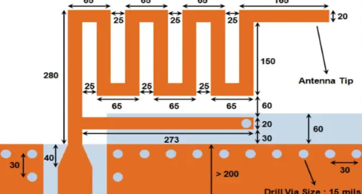
  • Examples: Microstrip patch, inverted-F (IFA), meandered monopole.
  • Advantages: Low cost, compact size, easy integration.
  • Challenges: Sensitive to PCB material, nearby components, and ground plane effects.
  1. External Antennas (Off-PCB Antennas)
  • Examples: Dipole, chip antennas with external radiators, PCB-trace antennas with external matching.
  • Advantages: Better radiation efficiency, less PCB dependency.
  • Challenges: Requires proper impedance matching and mechanical mounting.

The choice of antenna type influences PCB layout and routing strategies.

Contact us for PCB quote now |

3. Key PCB Layout Requirements for WiFi Antennas

3.1 Antenna Placement and Clearance

  • Keep-Out Zone: Maintain a clearance area (typically λ/4 or more) around the antenna to prevent detuning and performance degradation.
  • Ground Plane Considerations:
  • For monopole antennas, ensure an adequate ground plane beneath the antenna.
  • For dipole or balanced antennas, avoid asymmetric ground planes that distort radiation patterns.
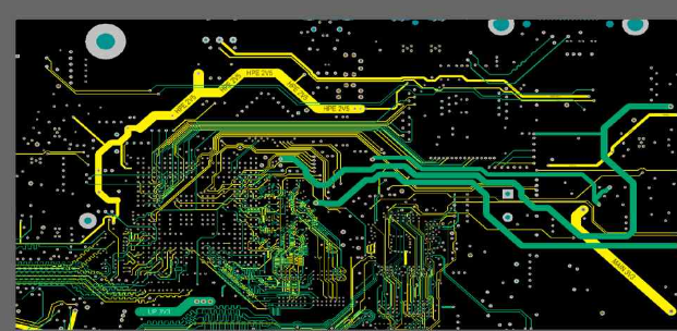
  • Proximity to Other Components:
  • Keep high-speed digital traces, power supplies, and noisy components (e.g., switching regulators) away from the antenna.
  • Avoid placing metal shields or large components near the antenna.

3.2 Impedance Matching and Trace Routing

  • 50Ω Transmission Line:
  • Use controlled impedance traces (microstrip or coplanar waveguide) to match the antenna’s 50Ω impedance.
  • Maintain uniform trace width and avoid sharp bends (use curved or 45° bends instead of 90°).
  • Minimize Stubs and Discontinuities:
  • Avoid vias in the RF path; if necessary, use back-drilled or buried vias.
  • Keep RF traces as short as possible to reduce losses.
  • Differential Pair Routing (for MIMO Antennas):
  • Ensure equal trace lengths for multiple antennas to maintain phase coherence.

3.3 Layer Stackup and Material Selection

  • PCB Substrate:
  • Use low-loss dielectric materials (e.g., Rogers RO4003C, FR-4 with controlled Dk/DF).
  • Avoid high-loss materials that degrade RF performance.
  • Ground Plane Integrity:
  • Ensure a solid ground plane beneath RF traces to minimize parasitic radiation.
  • Avoid splits or slots in the ground plane near the antenna.
Contact us for PCB quote now |

4. Structural and Mechanical Considerations

4.1 Enclosure Design and Antenna Placement

  • Plastic vs. Metal Enclosures:
  • Plastic enclosures are preferred for WiFi antennas due to minimal RF interference.
  • If a metal enclosure is used, ensure proper antenna placement (e.g., near an opening or with a radome).
  • Antenna Orientation:
  • Position the antenna for optimal polarization (vertical for most WiFi applications).
  • Avoid placing antennas near large metal objects or batteries that can block signals.

4.2 Environmental Factors

  • Thermal and Humidity Effects:
  • Ensure antenna materials can withstand operating temperatures and humidity without performance degradation.
  • Vibration and Mechanical Stress:
  • Secure antennas firmly to prevent movement-induced detuning.

5. Testing and Validation

  • Impedance Matching (VSWR Measurement):
  • Verify that the antenna’s VSWR is < 2:1 across the operating frequency band (e.g., 2.4GHz/5GHz for WiFi).
  • Radiation Pattern Testing:
  • Use an anechoic chamber to measure antenna gain and radiation efficiency.
  • Real-World Performance Testing:
  • Conduct throughput, range, and interference tests in actual deployment scenarios.

6. Conclusion

Designing a PCB with an integrated or external WiFi antenna requires careful attention to layout, routing, and mechanical constraints. Key takeaways include:

  • Maintaining proper clearance and ground plane integrity.
  • Using controlled impedance traces and minimizing RF discontinuities.
  • Selecting appropriate enclosure materials and antenna placement.
  • Validating performance through impedance matching and radiation testing.

By following these guidelines, engineers can ensure robust WiFi connectivity in their PCB-based wireless systems

Contact us for PCB quote now |
Post Tags: #4 layer pcb#aluminum clad pcb#aluminum core pcb#aluminum pcb#WiFi Antenna Requirements for PCB

Post navigation

Previous Previous
How to Improve Thermal Management Through PCB Design
NextContinue
PCB and BOM Design for Manufacturability (DFM) Analysis

Search

Search

Products

  • HDI Multilayer PCB
  • Rigid Flex PCB
  • Flex pcb
  • High Frequency PCB
  • High speed pcb
  • Heavy copper PCB
  • Metal Core PCB
  • Ceramic PCB

Address

Andwin Circuits Co.,Limited
Email: sales@andwinpcb.com
Tel: +86 755 2832 9394
Fax:+86 755 2992  6717
ADD:1-2F-1217,HouDeQun Industrial park,
NanTing RD NO.56,ShaJing,BaoAn,Shenzhen 518104,GuangDong,China

Products

  • HDI Multilayer PCB
  • Rigid Flex PCB
  • Flex pcb
  • High Frequency PCB
  • High speed pcb
  • Heavy copper PCB
  • Metal Core PCB
  • Ceramic PCB

Technology

  • Blogs
  • Via in pad
  • PCB E-test
  • PCB stack up
  • Metal core PCB panelization
  • Controlled impedance PCB

CERTIFICATION

Certification >>


Copyright© 2003 - 2026 Andwin | All Rights Reserved | Powered by Andwin

Scroll to top
  • Home
  • Products
    • HDI multilayer PCB
    • Rigid Flex PCB
    • Flex pcb
    • Special PCB
      • High Frequency PCB
        • Rogers RO4350B PCB
        • Rogers RO4003 pcb
        • Rogers RO3003 PCB
        • Rogers 5880 PCB
        • DICLAD 527 PCB
        • Taconic TLX series
        • Taconic TLX-8 RF PCB
        • Taconic TLX-9 RF PCB
      • High speed pcb
        • Megtron 6 High Speed PCB
        • TU-872 SLK Sp High Speed
      • High TG PCB
        • SHENGYI SH260 PCB
        • ISOLA 370HR PCB
        • ISOLA IS410 PCB
        • ISOLA IS420 PCB
      • Heavy copper PCB
      • Copper coin pcb
      • Copper inlay PCB
    • Metal Core PCB
      • Copper core pcb
      • Aluminum PCB
      • 2 Layers Aluminum PCB
      • Direct thermal MCPCB
      • 2 Layers Direct Thermal
    • Ceramic PCB
      • DPC ceramic PCB
      • DBC ceramic PCB
      • Thick film Ceramic PCB
      • Al2O3 Alumina PCB
      • AIN ALN ceramic PCB
      • IGBT Ceramic PCB
  • Service
    • PCB Assembly
    • Quick turn PCB assembly
    • PCBA conformal coating
  • Industry
    • Telecommunication
    • IoT and Wireless
    • Industrial Control
    • Thermal management
    • Power and Energy
    • IC test board
    • Automative
    • Medical
  • Capability
    • Rigid PCB
    • Rigid flex PCB
    • Metal core PCB
    • PCB Assembly
  • Technology
    • Blogs
    • Via in pad
    • PCB E-test
    • PCB stack up
    • MCPCB panelization
    • Controlled impedance PCB
  • About
    • About us
    • Certification
    • Factory Tour
  • Contact
Search