Safety Spacing Issues in PCB Design: A Comprehensive Analysis
Introduction
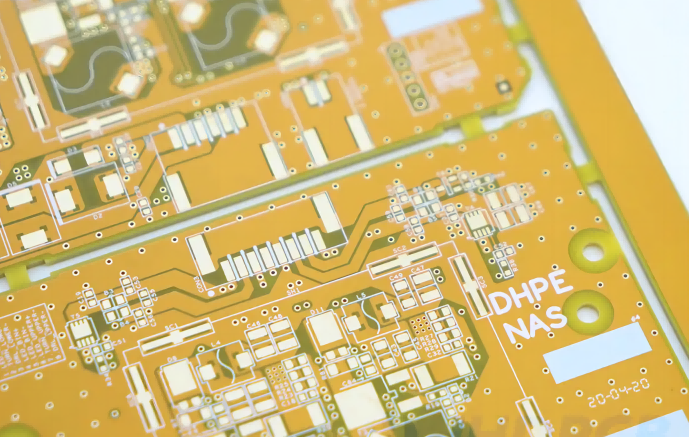
Printed Circuit Board (PCB) design is a complex process that requires careful consideration of numerous factors to ensure proper functionality, reliability, and safety. Among these considerations, safety spacing—the appropriate distances between various PCB elements—plays a critical role in determining the board’s performance and longevity. This 2000-word article examines the key safety spacing issues encountered in PCB design, their implications, and best practices for addressing them.
1. Fundamental Spacing Concepts in PCB Design
1.1 Definition of Safety Spacing
Safety spacing in PCB design refers to the minimum required distances between:
- Conductors (traces)
- Components
- Copper features
- Board edges
- Different voltage domains
These spacings are essential for preventing electrical, thermal, and mechanical issues that could compromise the board’s functionality or safety.
1.2 Importance of Proper Spacing
Appropriate spacing ensures:
- Prevention of electrical shorts and arcing
- Adequate insulation between conductors
- Proper heat dissipation
- Manufacturability and reliability
- Compliance with safety standards

2. Key Safety Spacing Issues in PCB Design
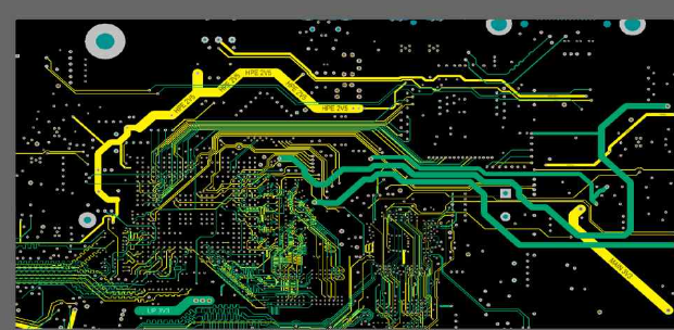
2.1 Trace-to-Trace Spacing
One of the most fundamental spacing considerations involves the distance between adjacent traces. Insufficient spacing can lead to:
Electrical Issues:
- Cross-talk and signal interference
- Potential short circuits
- Voltage breakdown in high-voltage applications
Design Factors Affecting Trace Spacing:
- Voltage difference between traces
- Signal frequency and rise time
- Environmental conditions (humidity, contamination)
- Insulating material properties
General Guidelines:
- Low-voltage digital signals: 0.15-0.20 mm (6-8 mil)
- Analog signals: 0.25-0.30 mm (10-12 mil)
- High-voltage applications: ≥1 mm (40 mil) or more depending on voltage
2.2 Component-to-Component Spacing
Proper spacing between components affects assembly, maintenance, and thermal performance:
Common Problems from Inadequate Component Spacing:
- Soldering difficulties during assembly
- Restricted access for rework and debugging
- Heat accumulation leading to thermal stress
- Electromagnetic interference between components
Recommended Practices:
- Maintain at least 0.5 mm (20 mil) between small passive components
- Allow 1-2 mm (40-80 mil) between larger components
- Provide additional space for heat-generating components
2.3 Copper-to-Edge Spacing
The distance between copper features (traces, pads, pours) and the board edge is critical for:
Manufacturing Considerations:
- Preventing copper tearing during board routing
- Ensuring proper plating at board edges
- Accommodating panelization and depaneling processes
Safety Requirements:
- Protection against edge arcing
- Prevention of conductive contamination reaching edges
Typical Requirements:
- Standard designs: 0.25-0.50 mm (10-20 mil)
- High-voltage designs: ≥1.0 mm (40 mil)
- UL certification often requires specific edge clearances
2.4 High-Voltage Spacing Considerations
High-voltage PCBs present unique spacing challenges:
Clearance and Creepage Requirements:
- Clearance: Shortest air path between conductors
- Creepage: Shortest path along insulation surface
Factors Influencing HV Spacing:
- Working voltage and transient overvoltages
- Pollution degree of operating environment
- Material group (Comparative Tracking Index)
- Altitude of operation (affects air dielectric strength)
Standards Compliance:
- IPC-2221 for general PCB spacing
- IEC 60950 for IT equipment
- IEC 60601 for medical devices
- Industry-specific standards (automotive, aerospace, etc.)
2.5 Spacing for High-Frequency Designs
High-frequency PCBs require special spacing considerations:
Signal Integrity Issues:
- Controlled impedance requirements
- Minimizing cross-talk between traces
- Proper grounding and return paths
Key Techniques:
- Increased spacing between critical signals
- Use of guard traces or ground planes
- Careful management of dielectric spacing
3. Manufacturing-Related Spacing Constraints
3.1 Fabrication Tolerances
Designers must account for manufacturing variations:
Common Tolerance Issues:
- Etching process variations affecting trace width
- Layer-to-layer registration in multilayer boards
- Drill wander in plated through-holes
Design for Manufacturing (DFM) Guidelines:
- Add tolerance margins to minimum spacings
- Consult with fabricator about their capabilities
- Consider worst-case scenarios in spacing calculations
3.2 Solder Mask Considerations
Solder mask affects effective spacing:
Solder Mask Bridging:
- Inadequate mask between pads can cause solder bridges
- Mask dams should be ≥0.1 mm (4 mil) for reliable application
Solder Mask Registration:
- Alignment tolerances may reduce effective clearance
- Design with mask misregistration in mind
4. Thermal Spacing Issues
4.1 Heat Dissipation Requirements
Proper spacing aids thermal management:
Thermal Spacing Guidelines:
- Additional space around high-power components
- Clearance for heat sinks and cooling features
- Thermal relief connections for ground/power planes
4.2 Thermal Expansion Considerations
Different expansion rates affect spacing:
CTE (Coefficient of Thermal Expansion) Effects:
- Material mismatches can cause mechanical stress
- Allow space for movement in high-temperature applications
5. Testing and Verification of Safety Spacing
5.1 Design Rule Checking (DRC)
Modern EDA tools provide automated spacing verification:
DRC Capabilities:
- Minimum spacing rules for all design elements
- Layer-specific spacing requirements
- Differential pair and high-speed rules
5.2 Electrical Rule Checking (ERC)
Additional verification for electrical safety:
ERC Functions:
- Voltage domain crossing checks
- High-potential isolation verification
- Return path analysis
6. Special Case Spacing Considerations
6.1 Mixed-Signal Design Spacing
Combining analog and digital signals requires:
Isolation Techniques:
- Physical separation of analog and digital sections
- Proper grounding strategies
- Use of moats and bridges in ground planes
6.2 RF and Microwave Design
Unique requirements for high-frequency designs:
Critical Spacing Parameters:
- Transmission line dimensions
- Antenna clearances
- Shielding requirements
7. Industry Standards and Regulatory Requirements
Various standards dictate spacing requirements:
7.1 IPC Standards
- IPC-2221: Generic Standard on Printed Board Design
- IPC-7351: Land Pattern Standards
- IPC-6012: Qualification and Performance Specification
7.2 International Safety Standards
- UL requirements for spacing
- IEC standards for various product categories
- Regional regulations (CE, FCC, etc.)
8. Best Practices for Managing Safety Spacing
8.1 Early Consideration in Design Flow
- Establish spacing requirements at schematic stage
- Document critical spacing needs
- Communicate with all stakeholders
8.2 Hierarchical Approach to Spacing Rules
- Define different spacing classes
- Implement rule hierarchies in EDA tools
- Prioritize critical spacings
8.3 Documentation and Version Control
- Maintain clear design rules documentation
- Track spacing requirement changes
- Archive design rule check reports
9. Future Trends in PCB Spacing
9.1 Miniaturization Challenges
- Balancing reduced spacing with reliability
- Advanced materials enabling closer spacing
- 3D packaging implications
9.2 Automation in Spacing Verification
- AI-assisted design rule checking
- Real-time spacing analysis
- Cloud-based rule management
Conclusion
Safety spacing in PCB design represents a critical balance between miniaturization demands and reliability requirements. By understanding the various spacing considerations—from basic trace-to-trace clearances to complex high-voltage isolation requirements—designers can create boards that are both compact and reliable. As PCB technology continues to evolve, with increasing density and higher performance requirements, the importance of proper safety spacing only grows more significant. Implementing robust spacing practices, leveraging modern design tools, and staying current with industry standards will remain essential for successful PCB design in all applications.