Mastering the Art of Complex PCB Layout: A Comprehensive Guide
Introduction
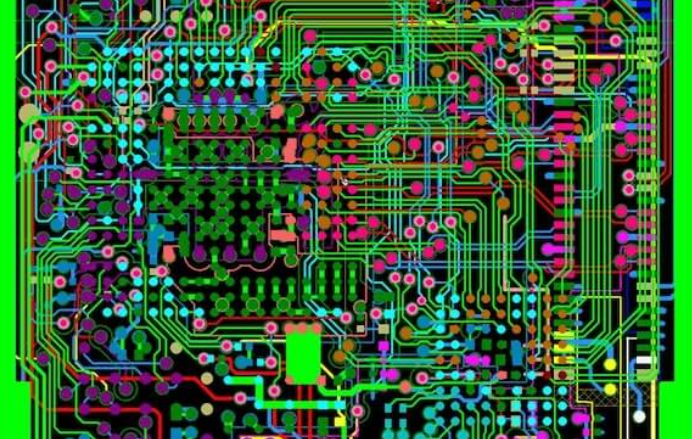
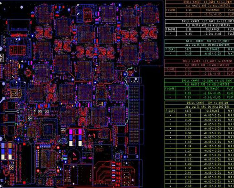
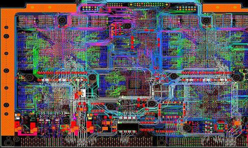
In today’s rapidly evolving electronics industry, Printed Circuit Board (PCB) design has become increasingly complex. With higher component densities, faster signal speeds, and more stringent performance requirements, PCB layout has transformed from a simple component placement exercise to a sophisticated engineering challenge. This 2000-word guide will explore the essential strategies and techniques for effectively laying out complex PCBs, addressing everything from initial planning to final verification.
Understanding the Complexity in Modern PCBs
Before diving into layout techniques, it’s crucial to understand what makes a PCB “complex.” Modern complex PCBs typically feature:
- High component density with fine-pitch packages (0.4mm or less)
- Mixed-signal designs combining analog, digital, and RF circuits
- High-speed interfaces (DDR memory, PCIe, USB 3.0+, etc.)
- Multiple voltage domains with strict power sequencing requirements
- Thermal management challenges from high-power components
- EMI/EMC compliance requirements
- Mechanical constraints and form factor limitations
These factors combine to create a multidimensional optimization problem where decisions in one area affect performance in others.

Pre-Layout Planning: The Foundation of Success
1. Schematic Review and Design Validation
A thorough schematic review is the critical first step in complex PCB layout:
- Verify component selections and footprints
- Check power network architecture and current requirements
- Identify critical signal paths and timing relationships
- Document design constraints and special requirements
2. Board Stackup Design
The layer stackup profoundly impacts signal integrity, power delivery, and manufacturability:
- Determine the number of layers needed based on complexity
- Plan signal layer arrangements (microstrip vs. stripline)
- Design proper power and ground plane structures
- Consider dielectric materials for high-frequency applications
- Account for controlled impedance requirements
3. Constraint Definition
Establishing clear design constraints early prevents costly rework:
- Electrical constraints (trace width, spacing, impedance)
- Physical constraints (component keepouts, height restrictions)
- Manufacturing constraints (DFM rules)
- Testability requirements
Component Placement Strategies
1. Functional Block Partitioning
Divide the board into logical functional blocks:
- Group related components together
- Consider signal flow between blocks
- Plan for proper isolation between sensitive circuits
- Account for thermal interactions
2. Hierarchical Placement Approach
Implement a structured placement methodology:
- Place connectors and mechanical components first
- Position primary ICs and processors
- Arrange supporting components (decoupling, termination)
- Place passive components and discrete circuitry
3. Critical Component Placement
Give priority to components with strict requirements:
- High-speed processors and memory devices
- Precision analog components
- RF circuitry
- Thermal-generating components
- Components with mechanical constraints
4. Power Delivery Network (PDN) Considerations
Power distribution affects placement decisions:
- Position voltage regulators close to their loads
- Consider current paths and loop areas
- Plan for adequate decoupling capacitor placement
- Account for voltage drop across the board

Routing Techniques for Complex PCBs
1. Signal Integrity-Conscious Routing
High-speed signals require special attention:
- Maintain proper impedance control
- Minimize via transitions on critical paths
- Implement length matching for parallel buses
- Avoid sharp angles and unnecessary bends
- Route differential pairs with proper coupling
2. Power Distribution Routing
Effective power delivery is essential:
- Use dedicated power planes where possible
- Implement proper plane splitting for multiple voltages
- Ensure adequate copper for high-current paths
- Consider via stitching for low-impedance connections
3. Mixed-Signal Routing Techniques
Prevent interference between analog and digital sections:
- Implement proper grounding strategies (star ground, partitioned planes)
- Route sensitive analog traces first
- Maintain adequate separation between signal types
- Use guard traces or ground shielding when necessary
4. EMI Reduction Techniques
Proactively address electromagnetic compatibility:
- Minimize loop areas in high-current paths
- Implement proper filtering at board interfaces
- Consider edge radiation and board resonances
- Use ground stitching vias at board edges
Advanced Layout Considerations
1. High-Density Interconnect (HDI) Techniques
For designs with extreme component density:
- Utilize microvias and buried vias
- Implement via-in-pad technology
- Consider sequential lamination processes
- Use thinner dielectric materials
2. Thermal Management Integration
Address heat dissipation in the layout:
- Identify hot components and plan heatsinking
- Incorporate thermal vias under high-power devices
- Consider copper pours for heat spreading
- Account for airflow in the final assembly
3. Design for Manufacturing (DFM)
Ensure the design can be reliably produced:
- Adhere to manufacturer’s capability guidelines
- Provide adequate spacing for assembly processes
- Consider test point accessibility
- Implement proper solder mask definitions
4. Design for Test (DFT)
Facilitate post-production testing:
- Include test points for critical signals
- Consider boundary scan requirements
- Plan for in-circuit test access
- Provide calibration and adjustment access

Verification and Validation
1. Design Rule Checking (DRC)
Perform comprehensive rule verification:
- Electrical rule checks
- Physical rule checks
- Manufacturing rule checks
- Assembly rule checks
2. Signal Integrity Analysis
Simulate and verify critical signals:
- Transmission line analysis
- Crosstalk evaluation
- Timing verification
- Power integrity analysis
3. 3D Mechanical Verification
Check for physical conflicts:
- Component clearance checks
- Assembly interference verification
- Enclosure compatibility
- Connector alignment
Tools and Technologies for Complex PCB Layout
Modern PCB design requires sophisticated tools:
- Advanced PCB design software with 3D capabilities
- Signal integrity analysis tools
- Thermal simulation packages
- Version control and collaboration systems
- Automated verification tools
Best Practices for Efficient Complex PCB Layout
- Maintain Design Discipline: Follow consistent naming conventions, layer usage, and organizational schemes.
- Document Everything: Create detailed layout guidelines and maintain design notes.
- Implement Modular Design: Reuse verified circuit blocks where possible.
- Plan for Iteration: Complex designs rarely work perfectly on the first try.
- Collaborate Early: Involve manufacturing and mechanical teams during layout.
- Validate Continuously: Perform checks throughout the process, not just at the end.
Conclusion
Laying out complex PCBs requires a systematic approach that balances electrical performance, physical constraints, and manufacturability. By following the strategies outlined in this guide—thorough planning, methodical component placement, careful routing, and comprehensive verification—designers can successfully navigate the challenges of complex PCB layout. Remember that each design presents unique requirements, and the most effective layouts come from applying fundamental principles while adapting to specific project needs.
As PCB technology continues to advance, staying current with new techniques, materials, and tools will be essential for tackling tomorrow’s layout challenges. The key to success lies in combining technical knowledge with practical experience and a disciplined approach to the design process.


