The Importance of Copper Thickness in PCB Manufacturing
Introduction
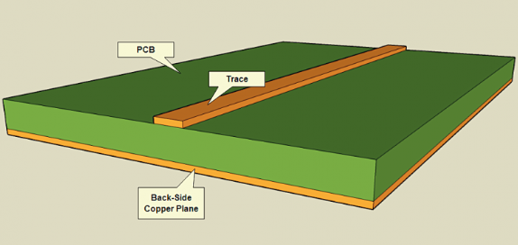
Printed Circuit Boards (PCBs) are the backbone of modern electronics, providing mechanical support and electrical connectivity for components. One of the most critical aspects of PCB design and manufacturing is copper thickness, which directly impacts the board’s performance, durability, and functionality. Copper is used to create conductive traces, pads, and planes that facilitate signal transmission and power distribution. The thickness of the copper layer affects electrical conductivity, thermal management, current-carrying capacity, and manufacturing yield.
This article explores the significance of copper thickness in PCB manufacturing, discussing its impact on electrical performance, thermal management, manufacturability, and reliability. We will also examine industry standards, measurement techniques, and considerations for selecting the appropriate copper weight for different applications.
1. Understanding Copper Thickness in PCBs
Copper thickness in PCBs is typically measured in ounces (oz) per square foot, representing the weight of copper spread over a one-square-foot area. Common copper weights include:
- 0.5 oz (17.5 µm) – Used in high-density, low-power applications.
- 1 oz (35 µm) – Standard for most consumer electronics.
- 2 oz (70 µm) – Used in power electronics and high-current applications.
- 3 oz (105 µm) and above – Found in heavy-duty applications like power supplies and motor controllers.
The choice of copper thickness depends on factors such as current requirements, thermal dissipation needs, and manufacturing constraints.
2. Impact of Copper Thickness on Electrical Performance
2.1 Current-Carrying Capacity
Copper thickness directly influences a PCB’s ability to carry current without excessive heating. According to IPC-2152 standards, thicker copper traces can handle higher currents due to lower resistance. For example:
- A 1 oz copper trace (10 mil width) can carry ~1A.
- A 2 oz copper trace (same width) can carry ~2.5A.
Insufficient copper thickness leads to increased resistive losses (I²R heating), potentially causing trace damage or failure.
2.2 Signal Integrity
High-speed and high-frequency PCBs require controlled impedance, which depends on trace geometry and copper thickness. Thinner copper is preferred for fine-pitch components, while thicker copper may require wider traces to maintain impedance, affecting routing density.
2.3 Resistance and Voltage Drop
Thicker copper reduces trace resistance, minimizing voltage drop across long traces—critical in power distribution networks.
3. Thermal Management Considerations
3.1 Heat Dissipation
Copper is an excellent thermal conductor. Thicker copper layers help dissipate heat from high-power components (e.g., CPUs, FPGAs, power MOSFETs), reducing the need for additional heatsinks.
3.2 Thermal Expansion
PCBs experience thermal cycling during operation. Copper thickness affects the coefficient of thermal expansion (CTE), influencing reliability in environments with temperature fluctuations.
4. Manufacturing and Fabrication Challenges
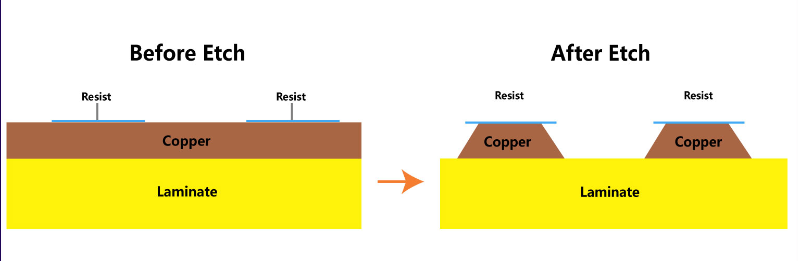
4.1 Etching and Trace Resolution
Thicker copper requires longer etching times, which can lead to undercutting and affect fine-pitch traces. Manufacturers must adjust etching parameters to maintain precision.
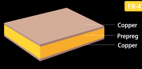
4.2 Layer Stackup and Impedance Control
Multilayer PCBs must balance copper thickness across layers to prevent warping and ensure consistent impedance.
4.3 Cost Implications
Thicker copper increases material costs and may require specialized fabrication techniques, impacting overall PCB cost.
5. Reliability and Durability
5.1 Mechanical Strength
Thicker copper improves mechanical robustness, reducing the risk of trace damage during handling or assembly.
5.2 Solder Joint Reliability
Proper copper thickness ensures sufficient thermal mass for reliable soldering, preventing cold joints or pad lifting.
6. Industry Standards and Measurement
- IPC-2221/2152: Guidelines for trace width and current capacity.
- IPC-6012: Qualification and performance specifications for rigid PCBs.
- Four-Point Probe Method: Used to measure copper thickness accurately.
7. Choosing the Right Copper Thickness
Selecting copper thickness involves trade-offs:
- High-current designs: Prefer 2 oz or thicker copper.
- High-density interconnects (HDI): Use 0.5 oz–1 oz for fine traces.
- RF/microwave PCBs: Optimize for impedance control.
Conclusion
Copper thickness is a fundamental parameter in PCB design, affecting electrical performance, thermal management, manufacturability, and reliability. Engineers must carefully evaluate application requirements and manufacturing constraints to select the optimal copper weight. As electronics evolve toward higher power and miniaturization, understanding copper thickness becomes even more critical for successful PCB fabrication.
By adhering to industry standards and leveraging advanced manufacturing techniques, designers can ensure that their PCBs meet performance and durability demands across various applications.