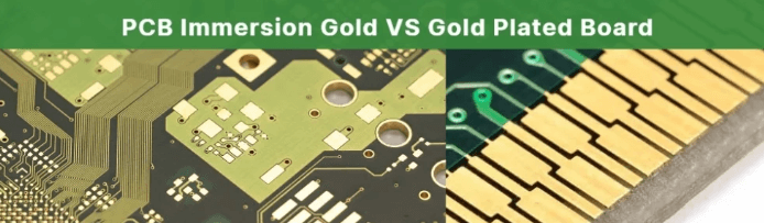
The Differences Between PCB Immersion Gold (ENIG) and Gold Plating (Electroplating)
Introduction
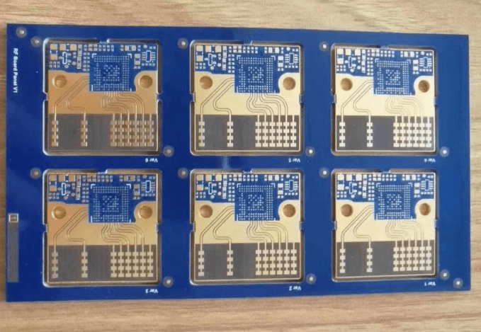
Printed Circuit Boards (PCBs) are essential components in modern electronics, providing the foundation for electrical connections between components. Among the various surface finishes available for PCBs, gold-based finishes are particularly important for their excellent conductivity, corrosion resistance, and reliability. The two primary gold-based surface finishes used in PCB manufacturing are Immersion Gold (also known as ENIG – Electroless Nickel Immersion Gold) and Gold Plating (electroplated gold). While both utilize gold as the surface material, they differ significantly in their manufacturing processes, properties, applications, and costs. This 2000-word article explores these differences in detail to help engineers and designers make informed decisions when selecting PCB surface finishes.
1. Process Differences
1.1 Immersion Gold (ENIG) Process
Immersion gold, or ENIG, is a two-layer metallic coating applied through a chemical process:
- Surface Preparation: The copper surface is cleaned and micro-etched to ensure proper adhesion.
- Nickel Deposition: An electroless nickel-phosphorus (Ni-P) layer (typically 3-6 μm thick) is chemically deposited on the copper.
- Immersion Gold: A thin layer of gold (typically 0.05-0.1 μm) is deposited on the nickel through a displacement reaction where gold ions replace nickel atoms at the surface.
The ENIG process is entirely chemical, requiring no electrical current, and results in a very uniform coating regardless of the circuit geometry.
1.2 Gold Plating Process
Gold plating, also called hard gold or electroplated gold, is an electrolytic process:
- Surface Preparation: Similar cleaning and micro-etching as ENIG.
- Nickel Underlayer: Often an electrolytic nickel layer (3-5 μm) is first deposited.
- Gold Electroplating: Using electrical current, gold ions are reduced onto the nickel surface from a plating solution. The thickness can vary significantly (0.5-3 μm or more for edge connectors).
Gold plating requires electrical connections to all areas being plated, which can complicate the process for complex boards. The thickness distribution depends on current density, leading to potential variations.
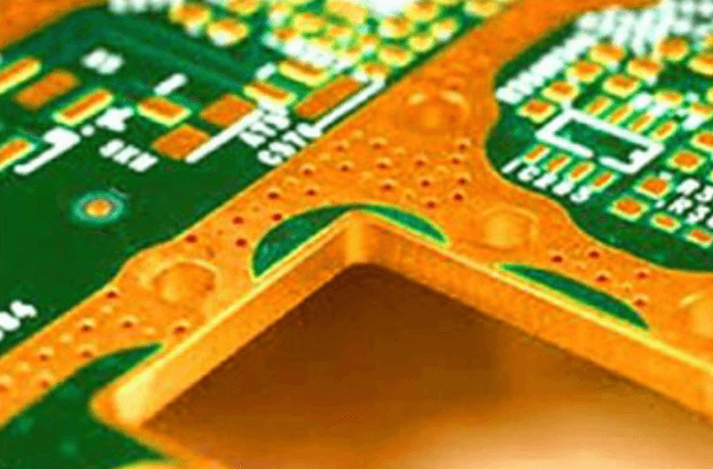
2. Thickness and Composition
2.1 Immersion Gold Characteristics
- Gold Thickness: Typically 0.05-0.1 μm (50-100 microinches)
- Nickel Layer: 3-6 μm
- Gold Purity: High purity (99.99% gold)
- Structure: The gold layer is porous at the atomic level due to the immersion process
2.2 Gold Plating Characteristics
- Gold Thickness: Can range from 0.5 μm to over 3 μm for edge connectors
- Nickel Layer: 3-5 μm
- Gold Purity: Often alloyed with cobalt or nickel (hard gold) for durability
- Structure: Denser, more continuous gold layer due to electrodeposition
3. Physical and Electrical Properties
3.1 Surface Hardness and Wear Resistance
- Immersion Gold: Softer surface (pure gold), more prone to scratches. Not suitable for frequent mechanical contact.
- Gold Plating: Harder surface (alloyed gold), excellent wear resistance. Ideal for contact points and connectors.
3.2 Solderability
- Immersion Gold: Excellent solderability due to fresh gold surface. The thin gold layer dissolves quickly into solder.
- Gold Plating: Thicker gold can lead to gold embrittlement if too much gold mixes with solder (typically >2.5 μm).
3.3 Electrical Conductivity
- Immersion Gold: Good conductivity, but the thin layer means most current passes through the nickel.
- Gold Plating: Excellent conductivity, especially for high-frequency applications.
3.4 Corrosion Resistance
- Immersion Gold: Excellent corrosion resistance due to complete gold coverage.
- Gold Plating: Superior corrosion resistance, especially with thicker gold layers.
4. Applications
4.1 Typical Uses for Immersion Gold
- Surface mount technology (SMT) applications
- Fine-pitch components (BGA, QFN, CSP)
- PCBs requiring flat surfaces (for good coplanarity)
- Applications needing excellent shelf life
- Boards with aluminum wire bonding
4.2 Typical Uses for Gold Plating
- Edge connectors and contact points
- Keyboards and membrane switches
- Test points requiring frequent probing
- High-reliability military and aerospace applications
- Gold wire bonding areas
5. Reliability Considerations
5.1 Black Pad Syndrome (ENIG)
A potential failure mode for immersion gold is “black pad” syndrome, where excessive phosphorus in the nickel layer or improper processing leads to a weak nickel-gold interface that can fracture during thermal cycling.
5.2 Nickel Corrosion (Gold Plating)
If the gold layer is too thin or porous in gold plating, nickel corrosion can occur over time, especially in harsh environments.
5.3 Thermal Stress Performance
- Immersion Gold: Generally good, but susceptible to black pad issues
- Gold Plating: Excellent thermal performance due to thicker, more robust gold layer
6. Cost Considerations
6.1 Immersion Gold Cost Factors
- Lower gold consumption (thin layer)
- Simpler process (no electrical connections needed)
- Generally less expensive than gold plating for most applications
6.2 Gold Plating Cost Factors
- Higher gold consumption (thicker layer)
- More complex process requiring electrical connections
- Additional masking often required
- Typically 30-50% more expensive than ENIG
7. Manufacturing Considerations
7.1 Immersion Gold Advantages
- Uniform coating regardless of geometry
- No electrical connections needed
- Suitable for complex, high-density designs
- Excellent for small features and tight tolerances
7.2 Gold Plating Challenges
- Requires electrical connections to all plating areas
- Thickness varies with current density (potential for non-uniformity)
- May require additional masking steps
- More difficult for complex geometries
8. Environmental Factors
8.1 Gold Usage
- Immersion gold uses significantly less gold, making it more environmentally friendly
- Gold plating consumes more gold, especially for thick deposits
8.2 Chemical Usage
- Both processes use chemicals that require proper handling and disposal
- Gold plating typically has more complex waste streams
9. Future Trends
9.1 Immersion Gold Developments
- Improved processes to prevent black pad syndrome
- Alternative nickel formulations for better reliability
- Thinner gold layers to reduce costs further
9.2 Gold Plating Innovations
- Selective plating techniques to reduce gold usage
- Improved hard gold formulations for better wear resistance
- Pulse plating for more uniform deposits
Conclusion
The choice between immersion gold (ENIG) and gold plating for PCB surface finishes depends on multiple factors including application requirements, cost considerations, and manufacturing constraints. Immersion gold offers an excellent balance of performance and cost for most standard applications, particularly those involving SMT components and requiring good shelf life. Gold plating, while more expensive, provides superior durability and is essential for applications involving mechanical contacts or requiring the highest reliability.
Understanding these differences enables PCB designers and engineers to select the most appropriate surface finish for their specific application, optimizing both performance and cost-effectiveness. As both technologies continue to evolve, we can expect further refinements that will enhance their respective advantages while mitigating current limitations.