Analysis of Copper-less Holes in PCBs and Improvement Methods
Abstract
Printed Circuit Boards (PCBs) are essential components in modern electronics, providing mechanical support and electrical connections for electronic components. One common defect in PCB manufacturing is the occurrence of copper-less holes (also known as “voids” or “non-plated through-holes”), which can lead to poor electrical conductivity and reliability issues. This paper analyzes the causes of copper-less holes in PCBs and proposes effective improvement methods to enhance manufacturing quality.
1. Introduction
PCB manufacturing involves multiple processes, including drilling, plating, etching, and soldering. Through-hole plating is crucial for establishing electrical connections between different layers of a PCB. However, defects such as copper-less holes can occur due to various factors, including improper drilling, plating issues, and contamination. These defects can result in open circuits, reduced signal integrity, and even PCB failure.
This paper examines the root causes of copper-less holes and discusses practical solutions to prevent and rectify them.
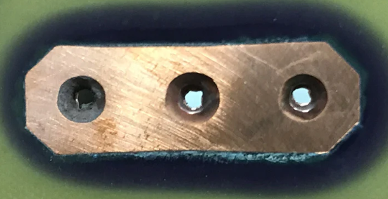
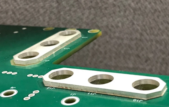
2. Causes of Copper-less Holes in PCBs
2.1 Poor Drilling Quality
- Drill Bit Wear: Worn-out drill bits can cause rough hole walls, leading to inadequate copper deposition.
- Incorrect Drilling Speed/Feed Rate: Excessive speed or improper feed rates can generate excessive heat, causing resin smear that blocks proper plating.
2.2 Inadequate Desmearing and Cleaning
- Resin Smear: During drilling, high temperatures can melt resin, which then smears over the hole walls, preventing proper copper adhesion.
- Contamination: Dust, grease, or residual chemicals can interfere with the plating process.
2.3 Electroless Copper Plating Issues
- Poor Activation: If the catalytic palladium-tin activator does not properly adhere to the hole walls, copper deposition will be insufficient.
- Insufficient Copper Deposition: Low bath concentration, improper temperature, or short plating time can lead to thin or missing copper layers.
2.4 Electroplating Defects
- Poor Current Distribution: Uneven current density during electroplating can result in inconsistent copper thickness or voids.
- Air Bubbles Trapped in Holes: Air pockets can prevent electrolyte contact, leading to unplated areas.
2.5 Material and Process Variations
- Low-Quality Substrates: Poor laminate materials may have inconsistent resin content, leading to plating issues.
- Improper Handling: Mechanical stress or contamination during handling can damage plated holes.
3. Improvement Methods
3.1 Optimizing Drilling Parameters
- Use sharp drill bits and replace them regularly.
- Adjust drilling speed and feed rate to minimize resin smear.
- Implement laser drilling for high-density interconnect (HDI) PCBs to reduce mechanical stress.
3.2 Enhancing Desmearing and Hole Preparation
- Apply plasma desmearing or chemical etching to clean hole walls effectively.
- Use proper rinsing and drying to remove contaminants before plating.
3.3 Improving Electroless Copper Plating
- Ensure proper activation by optimizing the palladium-tin catalyst bath.
- Monitor and adjust bath temperature, pH, and agitation for uniform deposition.
- Implement microetching before plating to enhance adhesion.
3.4 Enhancing Electroplating Uniformity
- Use pulse plating to improve copper distribution in high-aspect-ratio holes.
- Implement air agitation or solution circulation to prevent air bubbles.
- Optimize current density to avoid overplating or underplating.
3.5 Quality Control and Inspection
- Conduct automated optical inspection (AOI) to detect defects early.
- Perform cross-sectional analysis to verify plating thickness and uniformity.
- Implement electrical testing (e.g., flying probe testing) to ensure conductivity.
4. Conclusion
Copper-less holes in PCBs can significantly impact product reliability and performance. By identifying the root causes—such as drilling issues, poor desmearing, inadequate plating, and process variations—manufacturers can implement targeted improvements. Key solutions include optimizing drilling parameters, enhancing cleaning processes, improving plating techniques, and enforcing strict quality control measures.
By adopting these best practices, PCB manufacturers can minimize defects, improve yield rates, and ensure high-quality, reliable circuit boards for electronic applications.