How to Clone a PCB: A Comprehensive Guide
Introduction to PCB Cloning
Printed Circuit Board (PCB) cloning is the process of creating an exact or functional duplicate of an existing PCB. This practice is common in various industries for legitimate purposes such as legacy system maintenance, competitive analysis (where legal), and reverse engineering for repair or improvement. However, it’s important to note that PCB cloning may violate intellectual property laws if done without permission from the original designer.
This guide will walk you through the technical process of PCB cloning while emphasizing that this information should only be used for legal purposes such as repairing your own equipment, creating backup boards for systems where the original manufacturer no longer exists, or for educational understanding of PCB design.

Step 1: Preparation and Documentation
1.1 Gather Necessary Tools
Before beginning the cloning process, assemble the following tools:
- Digital camera or smartphone with high-resolution capability
- Magnifying glass or microscope (for small components)
- Multimeter
- LCR meter (for identifying passive components)
- Desoldering equipment (solder wick, desoldering pump)
- PCB design software (such as KiCad, Eagle, or Altium Designer)
- Graph paper or digital scanning equipment
1.2 Document the Original Board
Thorough documentation is crucial for accurate cloning:
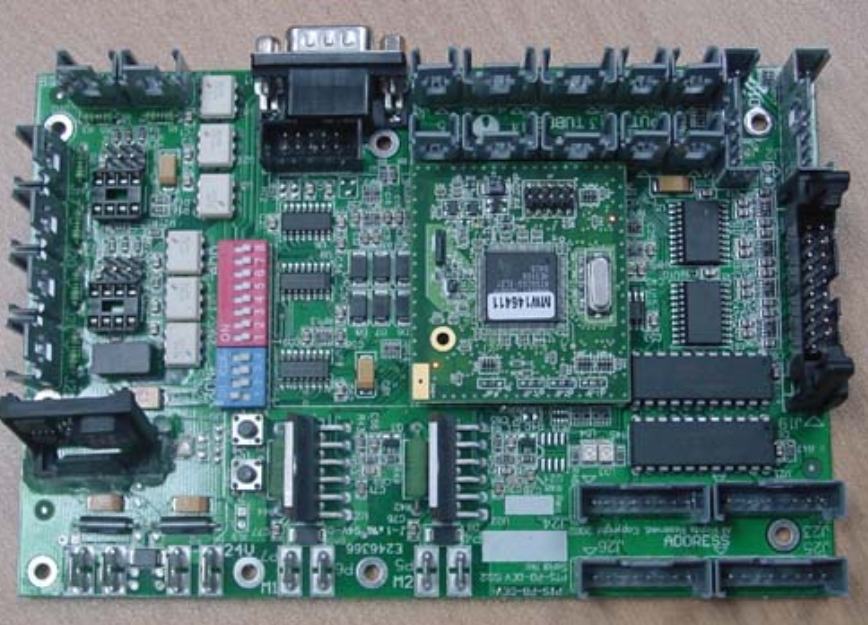
- Take high-resolution photographs of both sides of the PCB from directly above to minimize perspective distortion
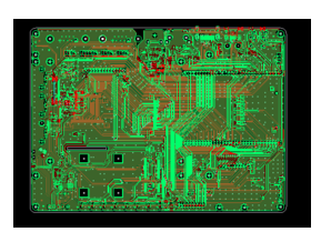
- For multilayer boards, document the layer structure by carefully examining vias and through-hole components
- Create a component list with reference designators (R1, C3, U5, etc.)
- Note any special markings, dates, or version numbers on the board
Step 2: Physical Analysis
2.1 Component Identification
- Create a bill of materials (BOM) by identifying each component:
- For ICs: Note part numbers, package types, and orientation
- For passives: Measure values using multimeter/LCR meter
- For connectors: Document pin counts and mechanical dimensions
- Record component placements and orientations:
- Note polarity of capacitors and diodes
- Document IC orientation (notch/dot positions)
2.2 Board Dimensions and Layer Count
- Measure the board’s physical dimensions precisely
- Determine layer count by:
- Examining edge connectors for visible layers
- Counting unique signal paths in through-hole vias
- Using bright light to trace internal layers (for simple boards)
Step 3: Schematic Recreation
3.1 Trace Mapping
- For single-layer boards:
- Use transparency sheets to trace connections
- Scan the board and trace connections in image editing software
- For double-layer boards:
- Document both sides separately then combine the connections
- Note vias that connect top and bottom layers
- For multilayer boards:
- Consider X-ray imaging (professional service may be needed)
- Use careful probing with continuity tester
3.2 Schematic Creation
- Enter all components into your PCB design software
- Recreate the schematic by:
- Following your trace documentation
- Grouping functional blocks logically
- Verifying connections with continuity tests
- Cross-check the schematic against the physical board multiple times
Step 4: PCB Layout Recreation
4.1 Board Outline and Mechanical Features
- Recreate the board outline with exact dimensions
- Document all mechanical features:
- Mounting holes
- Connector cutouts
- Any height restrictions
4.2 Component Placement
- Replicate the original component placement:
- Maintain same component orientations
- Preserve spatial relationships between components
- Note any obvious RF or high-speed design considerations
4.3 Trace Routing
- For simple boards:
- Manually route traces following your documentation
- Maintain original trace widths where visible
- For complex boards:
- Consider using autorouting with constraints
- Pay special attention to impedance-controlled traces
4.4 Layer Stackup Recreation
- For multilayer boards:
- Try to match original layer ordering
- Replicate via types (blind, buried, through)
- Match dielectric thicknesses if possible
Step 5: Verification and Testing
5.1 Design Rule Check (DRC)
- Run comprehensive DRC in your PCB software
- Verify against original board’s manufacturing capabilities
5.2 Prototype Fabrication
- Order prototype boards from a quick-turn PCB manufacturer
- Compare physical prototype with original:
- Layer-to-layer alignment
- Hole sizes and positions
- Silkscreen accuracy
5.3 Assembly and Functional Testing
- Populate the prototype with components
- Perform side-by-side testing with original board:
- Power-up characteristics
- Signal measurements at test points
- Functional performance comparison
Advanced Techniques for Complex Boards
6.1 Decapping ICs (for advanced reverse engineering)
- Chemical removal of IC packaging to examine die
- Microscopic examination of chip structure
- Only recommended for experts with proper equipment
6.2 X-ray Imaging
- Useful for examining:
- Multilayer board structures
- BGA component connections
- Internal board damage
6.3 Signal Analysis
- Use oscilloscopes and logic analyzers to:
- Capture timing diagrams
- Analyze communication protocols
- Verify signal integrity
Legal and Ethical Considerations
7.1 Intellectual Property Laws
- Copyright protection of PCB layouts
- Patent protection of circuit designs
- Trademark protection of branding
7.2 Permissible Uses of PCB Cloning
- Repair and maintenance of owned equipment
- Interoperability development (DMCA exemptions)
- Educational purposes
7.3 When to Consult Legal Counsel
- Before cloning for commercial purposes
- When original design protection status is unclear
- Before distributing cloned designs
Alternative Approaches
8.1 Clean Room Design
- Create functionally equivalent design without copying
- Implement same functionality through different means
8.2 Authorized Cloning
- Obtain permission from original designer
- License the design for reproduction
Conclusion
PCB cloning is a complex process that requires careful attention to detail, proper tools, and technical expertise. While the technical methods described here can produce accurate clones of existing boards, it’s crucial to consider the legal and ethical implications before proceeding with any cloning project. For legitimate purposes such as repair, maintenance, or educational study, PCB cloning can be a valuable skill that extends the life of electronic equipment and enhances understanding of electronic design.
Remember that in many cases, contacting the original manufacturer for replacement boards or design files may be more efficient and certainly more legal than attempting to clone a PCB. When done properly and ethically, PCB cloning can be an important tool in an engineer’s skillset for preserving and maintaining electronic systems.
Appendix: Recommended Tools and Resources
Software Tools:
- KiCad (Open source PCB design)
- Altium Designer (Professional-grade)
- Eagle (Popular for hobbyists)
- OpenCV (For image processing of board scans)
Hardware Tools:
- Digital microscope (Andonstar AD407)
- Fine-pitch soldering station (Hakko FX-888D)
- Precision multimeter (Fluke 87V)
- Portable X-ray systems (for advanced users)
Learning Resources:
- IPC standards for PCB design
- IEEE papers on reverse engineering techniques
- Online courses on PCB design and signal integrity