Why Does Poor Tin Plating Occur on PCBs? Causes and Solutions
Introduction
Printed Circuit Boards (PCBs) are essential components in modern electronics, providing mechanical support and electrical connections for various components. One critical process in PCB manufacturing is tin plating (soldering), which ensures reliable electrical conductivity and component attachment. However, poor tin plating (soldering defects) can lead to weak joints, electrical failures, and reduced product reliability.
This article explores the root causes of poor tin plating on PCBs, including material issues, process control problems, environmental factors, and design flaws. Additionally, we will discuss preventive measures and solutions to improve soldering quality.
1. Material-Related Causes
1.1 Poor Quality of PCB Surface Finish
The surface finish of a PCB (such as HASL, ENIG, OSP, or immersion tin) plays a crucial role in solderability. If the surface finish is contaminated, oxidized, or improperly applied, it can lead to poor wetting and weak solder joints.
- Oxidation: Copper pads exposed to air for too long can oxidize, preventing proper solder adhesion.
- Contamination: Oils, dust, or residues from manufacturing processes can interfere with solder bonding.
- Inconsistent Coating Thickness: Uneven plating (e.g., too thin or too thick) can cause poor solder wetting or bridging.
1.2 Low-Quality Solder Paste or Flux
- Expired or Contaminated Solder Paste: Solder paste with degraded flux activity or metal oxidation will not melt properly.
- Incorrect Solder Alloy Composition: Using the wrong alloy (e.g., lead-free vs. leaded) can affect melting temperature and wetting ability.
- Poor Flux Performance: Weak flux fails to remove oxides, leading to incomplete solder joints.
1.3 Substandard PCB Substrate
- Delamination or Blistering: Moisture absorption or thermal stress can cause PCB layers to separate, affecting plating adhesion.
- Poor Copper Adhesion: If the copper foil peels off easily, solder joints may fail under stress.
2. Process-Related Causes
2.1 Improper Stencil Design or Printing
- Incorrect Aperture Size: If stencil openings are too small or large, solder paste deposition will be uneven.
- Poor Alignment: Misaligned stenciling leads to insufficient or excessive solder paste on pads.
- Clogged Stencil: Dried solder paste residue can block apertures, causing incomplete prints.
2.2 Inadequate Reflow Soldering Profile
- Insufficient Preheat: Rapid heating can cause solder splattering or tombstoning.
- Excessive Peak Temperature: Overheating may damage components or oxidize solder.
- Incorrect Cooling Rate: Fast cooling can lead to brittle joints; slow cooling may cause excessive intermetallic growth.
2.3 Poor Wave Soldering Control
- Incorrect Wave Height: Too low results in weak joints; too high causes bridging.
- Improper Flux Application: Insufficient flux leads to poor wetting; excess flux leaves residues.
- Contaminated Solder Bath: Impurities (e.g., copper buildup) degrade solder quality.
2.4 Hand Soldering Issues
- Insufficient Heat or Time: Cold joints form when solder doesn’t fully melt.
- Excessive Heat: Overheating damages pads or components.
- Poor Technique: Inconsistent soldering leads to uneven joints.
3. Environmental and Handling Factors
3.1 Moisture Exposure
PCBs or components exposed to humidity may absorb moisture, leading to popcorning (internal vaporization during reflow) or oxidation.
3.2 Contamination from Handling
- Finger Oils or Dust: Skin contact or unclean workspaces introduce contaminants.
- Residues from Cleaning Agents: Improper cleaning leaves films that hinder soldering.
3.3 Storage Conditions
- Improper Packaging: PCBs stored in non-ESD or humid environments degrade over time.
- Exceeding Shelf Life: Surface finishes (e.g., OSP) degrade if stored too long before use.
4. Design-Related Causes
4.1 Poor Pad Geometry
- Too Small Pads: Insufficient area for proper solder adhesion.
- Incorrect Pad Spacing: Too close leads to bridging; too far causes weak joints.
4.2 Thermal Imbalance
- Uneven Heat Distribution: Large ground planes or heavy copper areas heat slower, causing tombstoning.
- Insufficient Thermal Relief: Poor heat dissipation leads to cold joints.
4.3 Inadequate Solder Mask Design
- Solder Mask Over Pads: Prevents proper solder wetting.
- Misaligned Solder Mask: Exposes unintended areas to solder.
5. Solutions to Prevent Poor Tin Plating
5.1 Material Improvements
- Use High-Quality Surface Finishes: ENIG or immersion silver for better solderability.
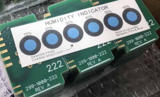
- Store PCBs Properly: Vacuum-sealed packaging with desiccants.
- Verify Solder Paste Quality: Check expiration dates and storage conditions.
5.2 Process Optimization
- Reflow Profile Tuning: Adjust preheat, soak, peak, and cooling phases.
- Stencil Maintenance: Regularly clean and inspect stencils.
- Automated Optical Inspection (AOI): Detect defects early in production.
5.3 Environmental Controls
- Humidity Control: Store PCBs in dry cabinets (<40% RH).
- Cleanroom Practices: Minimize contamination in assembly areas.
5.4 Design Best Practices
- Optimize Pad Layout: Ensure sufficient spacing and thermal relief.
- Use DFM (Design for Manufacturing): Collaborate with PCB manufacturers to avoid design flaws.
Conclusion
Poor tin plating on PCBs arises from multiple factors, including material defects, process errors, environmental exposure, and design shortcomings. By understanding these root causes, manufacturers can implement stricter quality controls, optimize soldering processes, and improve PCB designs to minimize defects. Ensuring high-quality solder joints is critical for the reliability and longevity of electronic products.
Through continuous improvement in materials, processes, and environmental management, the electronics industry can achieve higher yields and more robust PCB assemblies.