How to Optimize PCB Layout for Non-Isolated Switching Power Supplies
Introduction
The performance, efficiency, and reliability of non-isolated switching power supplies are heavily dependent on their printed circuit board (PCB) layout. Unlike isolated converters, non-isolated topologies (such as buck, boost, and buck-boost converters) present unique challenges in PCB design due to their high-frequency switching currents and tight coupling between components. A well-executed PCB layout can minimize electromagnetic interference (EMI), reduce power losses, improve thermal management, and enhance overall system stability.
This comprehensive guide explores the critical considerations and best practices for designing optimal PCB layouts for non-isolated switching power supplies, covering everything from component placement to grounding strategies and thermal management.
Fundamental Considerations
Understanding Current Paths
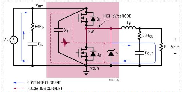
Non-isolated converters feature three primary current paths that must be carefully managed:
- High-frequency AC current paths: These carry pulsating currents between the switching node, inductor, and input/output capacitors
- DC input current paths: Deliver power from the input source to the converter
- DC output current paths: Supply regulated power to the load
The high-frequency AC paths are most critical as they generate the majority of EMI and can cause significant noise if not properly routed.
Switching Frequency Implications
Modern switching power supplies operate at frequencies ranging from hundreds of kHz to several MHz. These high frequencies:
- Create fast voltage and current transitions (high dV/dt and dI/dt)
- Generate significant electromagnetic fields
- Make parasitic capacitance and inductance more problematic
- Require careful attention to loop areas and impedance control
Component Placement Strategies
Power Stage Component Arrangement
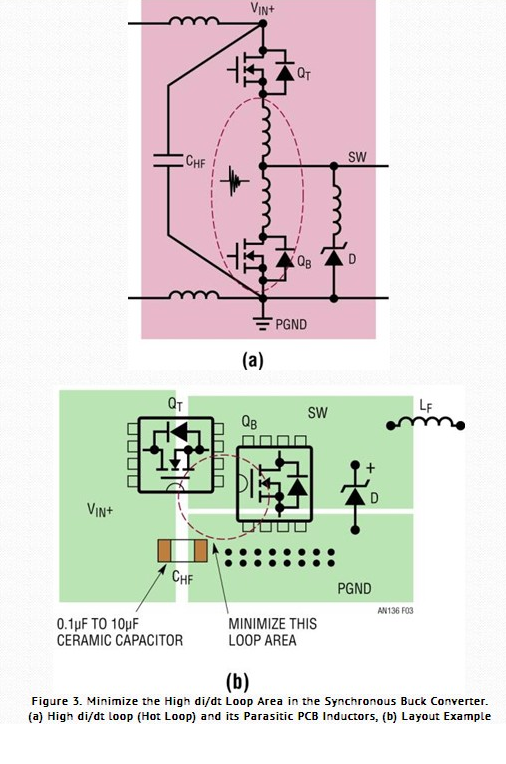
- Input capacitor placement:
- Position as close as possible to the IC’s VIN and GND pins
- Use multiple vias for low-impedance connections
- For multi-layer boards, place directly under the IC if space allows
- Switch node minimization:
- Keep the switching node (connection between switch, diode/sync FET, and inductor) as small as possible
- This reduces radiated EMI and switching losses
- Avoid using this node for routing other signals
- Inductor positioning:
- Place close to the IC’s SW pin and output capacitor
- Orient to minimize magnetic field coupling to sensitive circuits
- Consider shielding if in close proximity to noise-sensitive components
- Output capacitor placement:
- Position near the inductor and load
- Use multiple capacitors in parallel for optimal high-frequency and bulk filtering
Control Circuit Considerations
- Feedback network placement:
- Route feedback traces away from noisy areas (especially the switch node)
- Use Kelvin sensing for improved accuracy
- Keep feedback components close to the IC
- Compensation components:
- Place these near the IC’s compensation pin
- Avoid routing beneath or near switching nodes
- Bypass capacitors:
- Place small ceramic capacitors (typically 0.1µF to 1µF) very close to IC supply pins
- Use multiple vias for low-inductance connections
Routing Techniques
Power Traces
- Width and thickness:
- Calculate adequate trace widths based on current requirements
- Use thicker copper (2oz or more) for high-current designs
- Consider embedded bus bars for very high current applications
- Layer utilization:
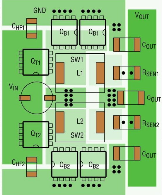
- Use multiple layers in parallel for high-current paths
- Maintain symmetry in parallel paths to ensure current sharing
- Via placement:
- Use multiple vias in parallel for high-current connections
- Place vias close to component pads
- Consider via-in-pad for critical connections
Signal Routing
- Sensitive signal protection:
- Route feedback and control signals away from power traces
- Use guard traces or ground shields for critical signals
- Minimize loop areas for all signal paths
- Crossing considerations:
- Avoid having sensitive signals cross power traces on adjacent layers
- If crossing is unavoidable, arrange at 90° angles
- Impedance control:
- Match trace lengths for differential signals
- Control impedance for high-speed control signals
Grounding Strategies
Ground Plane Implementation
- Single-point vs. multi-point grounding:
- Non-isolated converters typically benefit from a solid ground plane
- Maintain low-impedance connections throughout
- Ground plane segmentation:
- Generally avoid splitting the ground plane in non-isolated designs
- If separation is necessary, connect at a single point near the IC
- Noise-sensitive circuit grounding:
- Provide clean ground returns for control circuitry
- Avoid having sensitive signals return through high-current paths
Current Return Path Analysis
- Identify all current loops:
- Map out the high-frequency current paths
- Pay special attention to the input capacitor loop
- Minimize loop areas:
- Keep high di/dt loops as small as possible
- This reduces parasitic inductance and EMI radiation
- Layer stacking for return paths:
- Ensure adjacent signal layers have solid reference planes
- Maintain close coupling between signal and return paths
Thermal Management
Heat Dissipation Techniques
- Copper area utilization:
- Use large copper pours for heat spreading
- Incorporate thermal relief patterns where needed
- Via arrays for heat transfer:
- Implement thermal vias under hot components
- Connect to internal ground planes for additional heat sinking
- Component placement for airflow:
- Arrange components to facilitate natural convection
- Keep heat-generating components away from temperature-sensitive parts
Thermal Design Considerations
- Current density analysis:
- Ensure traces can handle expected current without excessive heating
- Consider temperature rise in trace width calculations
- Thermal pad design:
- Use appropriate pad sizes for power components
- Incorporate solder mask defined (SMD) or non-solder mask defined (NSMD) pads as appropriate
- Thermal simulation:
- Perform thermal analysis during layout
- Identify potential hot spots before fabrication
EMI Reduction Techniques
Layout-Based EMI Control
- Loop area minimization:
- The most effective way to reduce radiated emissions
- Pay special attention to the input capacitor loop
- Shielding strategies:
- Use grounded copper pours as shields
- Consider compartmentalization for sensitive areas
- Edge rate control:
- Implement layout techniques that support gate drive tuning
- Allow for series resistors in gate drive paths
Filter Implementation
- Input filter placement:
- Position input filters close to the power entry point
- Maintain proper grounding for filters
- Output filter considerations:
- Place output filters near the converter output
- Ensure low-inductance connections
- Component selection for EMI:
- Use low-ESR capacitors for effective filtering
- Select inductors with appropriate frequency characteristics
Design Verification
Layout Review Checklist
- Critical path verification:
- Confirm minimal switch node area
- Verify input capacitor placement
- Check inductor positioning
- Grounding inspection:
- Ensure solid ground connections
- Verify return paths for control signals
- Thermal assessment:
- Confirm adequate copper for heat dissipation
- Check via placement under hot components
Prototyping and Testing
- Initial bring-up procedures:
- Use current-limited supplies for first power-up
- Verify waveforms at critical nodes
- EMI testing preparation:
- Include test points for conducted emissions measurements
- Allow for additional filtering components if needed
- Thermal validation:
- Include temperature measurement points
- Plan for thermal imaging if possible
Advanced Techniques
Multi-Layer Board Strategies
- Layer stack-up optimization:
- Place power and ground planes adjacent for capacitance
- Arrange signal layers between reference planes
- Embedded components:
- Consider embedded passives for space savings
- Evaluate embedded magnetics for high-density designs
- 3D packaging considerations:
- Plan for component height restrictions
- Consider thermal expansion matching
High-Frequency Design (MHz+)
- Transmission line effects:
- Treat power traces as transmission lines at very high frequencies
- Implement proper termination where needed
- Parasitic minimization:
- Use interleaved winding techniques for planar magnetics
- Optimize pad sizes to minimize parasitic capacitance
- Material selection:
- Consider low-loss dielectric materials
- Evaluate high-frequency copper roughness effects
Common Pitfalls and Solutions
Frequent Layout Mistakes
- Overlooking return paths:
- Solution: Always analyze current return paths, especially for high-frequency components
- Inadequate input capacitor placement:
- Solution: Prioritize input capacitor positioning during initial placement
- Excessive switch node area:
- Solution: Keep SW node compact and avoid using it for routing other signals
Debugging Techniques
- Thermal imaging:
- Use to identify unexpected hot spots
- Verify current sharing in parallel components
- Near-field probing:
- Locate sources of EMI emissions
- Validate effectiveness of shielding techniques
- Loop inductance measurement:
- Use specialized equipment to quantify parasitic inductance
- Verify improvements after layout modifications
Conclusion
Optimizing the PCB layout for non-isolated switching power supplies requires careful consideration of current paths, component placement, grounding strategies, and thermal management. By implementing the techniques discussed in this guide—minimizing high-frequency loop areas, proper component positioning, effective grounding, and thorough design verification—engineers can create power supplies that achieve optimal performance, efficiency, and reliability.
Remember that each design presents unique challenges, and the best layouts often result from iterative refinement. Always allow time for prototyping and testing, as real-world performance may reveal opportunities for further optimization. With attention to these PCB layout principles, your non-isolated switching power supply designs will meet their technical requirements while minimizing EMI and thermal issues.