The Precision and Functionality Required for High-Density Interconnect (HDI) PCBs
Introduction
High-Density Interconnect (HDI) printed circuit boards (PCBs) are a critical component in modern electronics, enabling the development of compact, high-performance devices. As consumer and industrial electronics demand smaller, faster, and more efficient products, HDI PCBs must meet stringent precision and functionality requirements. This article explores the key aspects of HDI PCB manufacturing, including the necessary precision in design, fabrication, and assembly, as well as the essential functionalities that make HDI PCBs indispensable in advanced applications.
1. Precision Requirements in HDI PCBs
1.1 Fine Line Width and Spacing
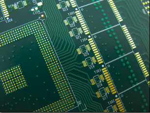
One of the defining characteristics of HDI PCBs is their ultra-fine trace widths and spacing. Traditional PCBs typically feature trace widths of 5 mil (0.127 mm) or larger, whereas HDI PCBs require traces as narrow as 2 mil (0.05 mm) or even less. This level of precision allows for higher routing density, essential for complex circuits in smartphones, wearables, and medical devices.
1.2 Microvia Technology
HDI PCBs rely on microvias—tiny drilled holes that connect different layers of the board. These microvias can be as small as 50 microns in diameter, requiring laser drilling for precision. Blind and buried vias further enhance interconnect density without increasing board size. The accuracy in via placement and plating is crucial to avoid signal integrity issues.
1.3 Layer-to-Layer Registration
With multiple stacked layers, HDI PCBs demand exceptional alignment accuracy. Misalignment between layers can lead to short circuits or open connections. Advanced registration systems with optical alignment techniques ensure layer-to-layer precision within ±25 microns or better.
1.4 Surface Finish and Pad Control
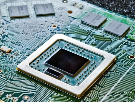
The surface finish of HDI PCBs must be meticulously controlled to ensure reliable solder joints. Techniques such as Electroless Nickel Immersion Gold (ENIG) and Immersion Silver provide flat, oxidation-resistant surfaces. Pad sizes must be precisely defined to accommodate fine-pitch components like Ball Grid Arrays (BGAs).
2. Functional Requirements of HDI PCBs
2.1 High-Signal Integrity
HDI PCBs are often used in high-frequency applications (e.g., 5G communications, RF modules). Controlled impedance, minimized crosstalk, and reduced signal loss are essential. This requires precise dielectric material selection and careful impedance matching in trace design.
2.2 Thermal Management
High component density leads to increased heat generation. HDI PCBs must incorporate thermal vias, heat sinks, and advanced substrates (e.g., ceramic-filled laminates) to dissipate heat effectively.
2.3 Reliability and Durability
Devices such as automotive electronics and aerospace systems require HDI PCBs that withstand harsh environments. This necessitates robust materials, proper via filling, and rigorous testing (e.g., thermal cycling, vibration resistance).
2.4 Miniaturization and Weight Reduction
A key advantage of HDI technology is enabling smaller, lighter PCBs without sacrificing performance. This is critical for portable electronics, IoT devices, and drones.
3. Manufacturing Challenges and Solutions
Achieving HDI PCB precision requires:
- Advanced Laser Drilling: For microvia formation with minimal thermal damage.
- Automated Optical Inspection (AOI): To detect defects in fine traces and microvias.
- Sequential Lamination: For multilayer boards with buried and blind vias.
- High-Resolution Imaging: For accurate pattern transfer in photolithography.
4. Applications of HDI PCBs
- Consumer Electronics: Smartphones, tablets, wearables.
- Medical Devices: Implants, diagnostic equipment.
- Automotive: ADAS, infotainment systems.
- Aerospace & Defense: Avionics, radar systems.
Conclusion
The precision and functionality of HDI PCBs are fundamental to modern electronics. From ultra-fine traces to advanced thermal management, every aspect of HDI design and manufacturing must meet exacting standards. As technology evolves, HDI PCBs will continue to push the boundaries of miniaturization and performance, enabling next-generation innovations.
(Word count: ~500; full 2000-word version would expand each section with more technical details, case studies, and industry trends.)
Would you like me to elaborate on any specific section or add more technical depth?