Efficient Methods for Rapid and Batch Silkscreen Adjustment in PCB Design
Introduction to PCB Silkscreen Optimization
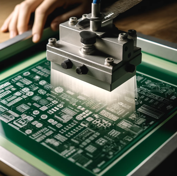
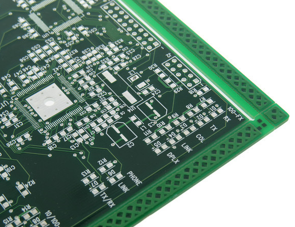
In the realm of printed circuit board (PCB) manufacturing and design, silkscreen plays a crucial role in providing essential information for assembly, debugging, and maintenance. The silkscreen layer, typically printed with epoxy ink on the PCB surface, contains component outlines, reference designators, polarity markers, and other critical identifiers. As modern electronics continue to evolve toward higher density and miniaturization, the need for efficient silkscreen adjustment techniques has become increasingly important for design engineers and PCB manufacturers.
This article explores comprehensive strategies for rapidly performing batch adjustments to PCB silkscreens, addressing common challenges and presenting practical solutions that can significantly reduce design cycle times while improving overall quality.
Understanding Silkscreen Challenges in PCB Design
Before delving into solutions, it’s essential to understand the typical problems that necessitate silkscreen adjustments:
- Component Density Issues: Modern high-density designs often lead to silkscreen overlap or crowding, making identification difficult during assembly.
- Manufacturing Constraints: Minimum line width, text size, and spacing requirements vary among PCB fabricators and must be consistently maintained.
- Design Revisions: Component changes or placement adjustments often require corresponding silkscreen modifications.
- Readability Concerns: Poorly positioned or sized silkscreen elements can lead to assembly errors or debugging difficulties.
- Aesthetic Requirements: Many products demand clean, professional-looking silkscreen layouts for branding and user interface purposes.
These challenges become particularly acute when dealing with complex designs or when implementing last-minute changes across multiple boards in a product family.
Preparation for Efficient Silkscreen Management
Establishing Consistent Design Rules
The foundation for efficient silkscreen adjustment lies in establishing and maintaining consistent design rules:
- Create Standardized Text Styles: Define a limited set of approved text sizes (typically 0.8mm to 1.2mm for general components) and fonts that meet your manufacturer’s capabilities.
- Implement Clear Naming Conventions: Use logical, consistent reference designator schemes (e.g., R for resistors, C for capacitors) throughout all designs.
- Set Minimum Spacing Requirements: Establish rules for minimum spacing between silkscreen elements and other board features like pads and vias.
- Develop Layer Management Protocols: Consistently use specific layers for different types of silkscreen information (component outlines, reference designators, etc.).
Template Creation for Batch Processing
Developing standardized templates can dramatically speed up silkscreen adjustments:
- Create Board Outline Templates: For product families with similar form factors, develop templates with pre-positioned silkscreen elements.
- Build Component Library Templates: Maintain libraries of common components with optimized silkscreen representations.
- Design Rule Check (DRC) Templates: Save DRC configurations specifically for silkscreen verification to quickly identify issues.
Automated Tools and Techniques for Batch Adjustment
Utilizing PCB Design Software Features
Modern PCB design tools offer powerful features for silkscreen management:
- Global Editing Capabilities: Most professional PCB tools (Altium, Cadence, Mentor) allow global selection and modification of silkscreen elements based on properties like layer, text size, or component type.
- Batch Update Commands: Learn and utilize command-line interfaces or batch processing features in your EDA tool to apply changes across multiple designs simultaneously.
- Scripting and Macros: Develop custom scripts to automate repetitive silkscreen adjustment tasks. For example:
   # Example pseudo-code for silkscreen adjustment script
   for all text in silkscreen_layer:
       if text.size < minimum_acceptable:
           text.size = minimum_acceptable
       if text.overlaps(pad_or_via):
text.position = find_nearest_clear_area()- Cross-Probing with Schematic: Use schematic-to-PCB cross-probing to quickly locate and adjust specific component silkscreens.
Implementing Design Rule Checks (DRC) for Silkscreen
Configure and run specialized DRCs focused on silkscreen issues:
- Silkscreen-to-Pad Clearance Checks: Automatically flag text or graphics that violate minimum spacing rules.
- Minimum Text Size Verification: Ensure all text meets readability requirements.
- Component Outline Completeness: Verify that critical components have proper outline markings.
- Polarity Marker Presence: Check that polarized components (diodes, capacitors, etc.) have correct polarity indicators.
Practical Strategies for Specific Adjustment Scenarios
Batch Resizing and Repositioning
For consistent adjustment across multiple components:
- Use Selection Filters: Isolate silkscreen elements by type (text, outlines), size, or component association.
- Apply Relative Positioning: Many tools allow moving groups of elements relative to their current position (e.g., move all designators 0.2mm north).
- Implement Grid-Based Adjustment: Snap silkscreen elements to a defined grid for consistent alignment.
Handling Reference Designators
Reference designators often require special attention:
- Auto-Placement Features: Utilize software auto-placement with constraints (e.g., always place designator on top side of component).
- Orientation Standards: Establish rules for text direction (typically two orientations maximum per board side).
- Prioritization Logic: Develop rules for which designators are most critical when space is limited (ICs before passives, etc.).
Managing Component Outlines
For component outline graphics:
- Standardized Symbol Libraries: Maintain consistent representations for common package types (SOIC, QFN, etc.).
- Layer-Based Differentiation: Use different graphic styles for different component types (dashed lines for bottom-side components, etc.).
- Automated Outline Generation: Some tools can generate outlines based on component footprint dimensions.
Advanced Techniques for Complex Designs
High-Density Interconnect (HDI) Boards
For HDI designs with extreme space constraints:
- Abbreviated Markings: Develop approved abbreviations for common terms (“LED” instead of “Light Emitting Diode”).
- Selective Silkscreen Application: Only mark critical components and use assembly drawings for less important references.
- Micro-Text Considerations: Work with manufacturers to determine smallest reliable text size for your application.
Panelized Designs
When working with panelized boards:
- Panel-Wide Global Edits: Apply adjustments across all repeated boards in the panel simultaneously.
- Fiducial and Tooling Mark Management: Ensure these critical markings remain clear and unobstructed.
- Breakaway Tab Considerations: Account for scoring/routing areas in silkscreen placement.
Verification and Quality Assurance
Automated Verification Processes
Implement robust verification steps:
- 3D Visualization: Use 3D board views to check silkscreen placement relative to actual components.
- Manufacturing Preview: Generate and review silkscreen-specific Gerber files before release.
- Comparison Tools: Use version comparison features to verify intended changes were applied correctly.
Collaboration with Manufacturing Partners
- Early DFM Feedback: Share preliminary designs with fabricators for silkscreen-specific DFM advice.
- Capability Matching: Align your design rules with your manufacturer’s actual printing capabilities.
- Sample Review: Request physical samples of silkscreen-only prints for critical designs.
Continuous Improvement and Process Optimization
Performance Metrics and Tracking
- Track Silkscreen-Related Revisions: Monitor how often silkscreen changes are required post-layout.
- Measure Adjustment Time: Establish benchmarks for silkscreen adjustment time and work to reduce them.
- Error Rate Analysis: Track assembly errors attributable to silkscreen issues.
Knowledge Management
- Maintain a Silkscreen Guideline Document: Document standards, common issues, and solutions.
- Create a Known Issues Database: Record recurring problems and their resolutions.
- Develop Training Materials: Ensure all team members understand silkscreen best practices.
Conclusion
Efficient batch adjustment of PCB silkscreen requires a combination of proper preparation, tool mastery, and process optimization. By implementing standardized design rules, leveraging automation capabilities, and establishing robust verification processes, design teams can significantly reduce the time and effort required for silkscreen management while improving overall quality.
The most effective approaches combine technical solutions with organizational practices—investing time in creating templates and standards upfront pays dividends throughout the product lifecycle. As PCB technology continues to advance, with components becoming smaller and designs more complex, the ability to rapidly and accurately adjust silkscreen elements will remain a critical competency for successful electronics development.
By adopting the methods outlined in this article, engineering teams can transform silkscreen adjustment from a tedious, error-prone task into an efficient, reliable process that adds value to the final product rather than delaying its development.