What Makes an Excellent PCB File: A Comprehensive Guide
Printed Circuit Board (PCB) design is both an art and a science, requiring technical expertise, attention to detail, and consideration of manufacturing realities. An excellent PCB file goes beyond mere functionality—it ensures manufacturability, reliability, and optimal performance while minimizing costs and potential issues. This 2000-word guide explores the essential characteristics that distinguish superior PCB files from average ones.
1. Proper File Organization and Documentation
Logical File Structure
An excellent PCB file begins with impeccable organization. The design package should include:
- A clear folder structure separating schematic files, layout files, fabrication outputs, and documentation
- Consistent naming conventions for all files (e.g., “ProjectName_Rev1.0_Schematic.pdf”)
- Version control information either embedded in filenames or through proper version control systems
Comprehensive Documentation
Superior PCB files always include:
- Readme files explaining any special requirements or considerations
- Assembly drawings with component placement, orientation markings, and reference designators
- Bill of Materials (BOM) with complete part numbers, manufacturers, and alternatives
- Layer stack-up documentation including materials, thicknesses, and copper weights
- Design constraints and rules that were applied during layout
- Testing procedures for verification and quality control
2. Design for Manufacturability (DFM) Compliance
Adherence to Manufacturer Capabilities
An excellent PCB designer always:
- Verifies the manufacturer’s capabilities (minimum trace/space, hole sizes, etc.) before starting
- Maintains appropriate clearances (typically 3-4 mil trace/space for standard designs)
- Uses standard drill sizes (avoiding odd sizes like 13.5 mil when 12 or 15 would work)
- Includes proper tolerances for critical dimensions
Panelization Considerations
For production runs:
- Includes appropriate panelization if required (with breakaway tabs or mouse bites)
- Provides adequate clearance between boards on the panel
- Includes fiducial marks and tooling holes when necessary
- Considers depaneling method (V-scoring, routing, etc.) in the design
3. Optimal Electrical Characteristics
Proper Signal Integrity
Excellent PCB files demonstrate:
- Appropriate trace widths for current carrying capacity (using IPC-2152 standards)
- Controlled impedance where needed (with clear documentation of target values)
- Proper high-speed design techniques (length matching, differential pairs, etc.)
- Minimized crosstalk through adequate spacing or ground shielding
Power Distribution
The design should feature:
- Adequate power plane coverage with proper copper balancing
- Appropriate decoupling capacitor placement (near power pins)
- Proper via sizing for current requirements in power nets
- Consideration of voltage drop across the board
4. Robust Mechanical Design
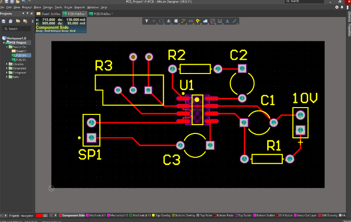
Component Placement
Superior layouts show:
- Logical grouping of related components
- Consideration of thermal management (spacing of heat-generating parts)
- Accessibility for testing and rework
- Proper clearance for mechanical parts (connectors, switches, etc.)
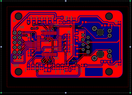
Board Outline and Mounting
Excellent designs include:
- Clear, accurate board outlines with all dimensions specified
- Proper mounting hole placement with adequate keep-out areas
- Consideration of mechanical stress points (like connectors)
- Clearance for any housings or enclosures
5. Comprehensive Verification
Design Rule Checking (DRC)
Before release, the file should pass:
- Electrical Rule Checking (ERC) for schematic errors
- Full Design Rule Checking with manufacturer-specific rules
- 3D collision checks (if applicable)
- Signal integrity simulations for critical nets
Cross-Validation
The excellent PCB file ensures:
- Consistency between schematic and layout (reference designators match)
- BOM matches placed components
- All nets are properly connected (no accidental airwires)
- All design constraints have been met
6. Proper Output Files
Fabrication Files
The complete package includes:
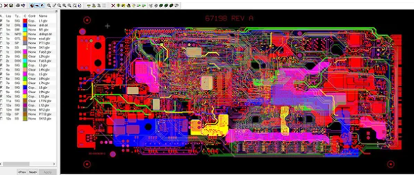
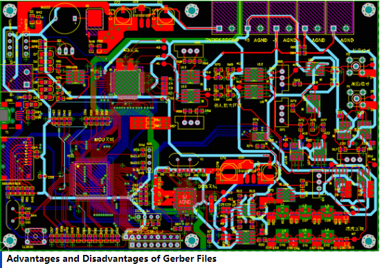
- Gerber files (RS-274X preferred) for all layers
- Drill files (Excellon format) with proper tool definitions
- IPC-356 netlist for verification
- Silk screen and solder mask files with proper clearances
Assembly Files
For manufacturing:
- Pick-and-place files with centroid data
- Solder paste stencil files (if applicable)
- Assembly drawings with orientation markings
- Test point files for automated testing
7. Design for Testability (DFT)
Excellent PCB files incorporate:
- Adequate test points for critical signals
- Proper spacing for test probes
- Consideration of in-circuit test (ICT) requirements
- Built-in self-test (BIST) capabilities where appropriate
8. Thermal Management
Superior designs address:
- Proper heat sinking for power components
- Thermal relief on pads connected to planes
- Adequate copper for heat dissipation
- Consideration of airflow in the final application
9. Compliance and Standards
The design should:
- Meet all applicable safety standards (UL, IEC, etc.)
- Comply with relevant EMC/EMI requirements
- Follow industry standards (IPC classifications)
- Include proper certification markings if required
10. Future-Proofing
Excellent PCB files consider:
- Potential design changes (test points for future modifications)
- Alternative component footprints where appropriate
- Documentation for easy revision
- Clear comments in design files explaining non-obvious decisions
Common Pitfalls to Avoid
Even experienced designers sometimes overlook:
- Silkscreen issues: Overlapping text, missing polarity markers, or unreadable sizes
- Solder mask problems: Inadequate clearance over pads or vias
- Incomplete design rules: Missing constraints for specific nets or areas
- Manufacturing mismatches: Designing for 6-layer boards when budget requires 4-layer
- Component availability: Specifying hard-to-get parts without alternatives
Tools for Creating Excellent PCB Files
While the designer’s skill matters most, quality tools help:
- Schematic capture: Altium, OrCAD, KiCad, Eagle
- PCB layout: Same as above plus Cadence Allegro, PADS
- Analysis tools: HyperLynx (SI/PI), Ansys SIwave, Keysight ADS
- Verification: Valor NPI, CAM350, Gerber viewers
- Version control: Git (with proper binary handling), SVN
The Human Factor
Technical excellence alone doesn’t guarantee an excellent PCB file. The best designers:
- Communicate clearly with all stakeholders (engineers, manufacturers, assemblers)
- Document decisions made during design (why certain tradeoffs were chosen)
- Seek feedback from manufacturing partners early in the process
- Review thoroughly before release (fresh eyes catch more errors)
- Learn continuously from each project’s successes and mistakes
Conclusion
An excellent PCB file represents the culmination of thoughtful design, rigorous verification, and clear communication. It balances electrical requirements with mechanical constraints, optimizes for manufacturability without sacrificing performance, and provides all necessary information for successful production. By focusing on the aspects outlined in this guide—from proper documentation to DFM compliance to thorough verification—designers can create PCB files that stand out for their quality, reliability, and professional execution.
The mark of truly excellent PCB design isn’t just a board that works, but one that can be manufactured consistently, tested effectively, and maintained easily throughout its product lifecycle. This holistic approach separates adequate PCB files from exceptional ones that become references for future designs.
Remember that in PCB design, perfection comes not from adding more features, but from eliminating all that is unnecessary while ensuring everything that remains works flawlessly together. This philosophy, applied diligently across all aspects of PCB file creation, is what ultimately defines excellence in the field.