Do you know the structure and function of PCB board?
Today’s PCB substrate is composed of three main components: copper foil, reinforcement, and epoxy. However, since the start of the lead-free process, the fourth powder (fillers) has been added to the PCB board in large quantities to improve the heat resistance of the PCB.
We can think of copper foil as blood vessels in the human body, which are used to transport important blood and allow the PCB to move; reinforcement can be thought of as bones in the human body, which are used to support and strengthen the PCB so that it does not fall down; and resin can be thought of as human muscles, which are the main components of the PCB.
Do you know the structure and function of PCB board?
The following will explain the uses, characteristics, and precautions of these four PCB materials:
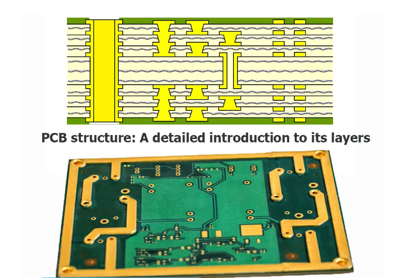
1.Copper Foil
Electric Circuit: Conductive circuit.
Signal line: Signal line that transmits information.
Vcc: Power layer, working voltage. The working voltage of the earliest electronic products was mostly set at 12V. With the evolution of technology and the requirement of power saving, the working voltage gradually became 5V, 3V, and now it is gradually moving towards 1V. Correspondingly, the requirements for copper foil are getting higher and higher.
GND (Grounding): Grounding layer. You can think of Vcc as a water tower in your home. When we turn on the faucet, water (electrons) will flow out through the water pressure (working voltage), because the operation of electronic components is determined by the flow of electrons; and GND can be imagined as a sewer. All used or unused water flows through the sewer. Otherwise, the faucet keeps draining water, and the house will be flooded.
Heat Dissipation (due to high thermal conductivity): Heat dissipation. Have you heard that some CPUs are so hot that they can cook eggs? This is not an exaggeration. Most electronic components consume energy and generate heat energy. At this time, it is necessary to design a large area of copper foil to release the heat energy into the air as soon as possible. Otherwise, not only humans can’t stand it, but even electronic components will crash.
2.Reinforcement
When selecting PCB reinforcement materials, the following excellent properties must be possessed. Most of the PCB reinforcement materials we see are made of glass fiber (GF, Glass Fiber). If you look closely, the material of glass fiber is a bit like a very thin fishing line. Because of the following individual advantages, it is often selected as the basic material of PCB.
High Stiffness: With high “rigidity”, the PCB is not easy to deform.
Dimension Stability: With good dimensional stability.
Low CTE: With low “thermal expansion coefficient”, it prevents the circuit contacts inside the PCB from detaching and causing failure.
Low Warpage: With low deformation, that is, low board bending and board warping.
High Modules: High “Young’s modulus”
3.Resin Matrix (resin mixture)
Traditional FR4 boards are mainly epoxy, while LF (Lead Free)/HF (Halogen Free) boards use a variety of resins and different curing agents, which increases the cost, about 20% for LF and about 45% for HF.
HF boards are brittle and easy to crack, and the water absorption rate increases. Thick and large boards are prone to CAF, so it is necessary to use open fiber cloth and flat fiber cloth instead, and strengthen the material with uniform impregnation.
Good resin must meet the following conditions:
Heat Resistance: Good heat resistance. After heating and welding for two to three times, the board will not explode, which is called good heat resistance.
Low Water Absorption: Low water absorption. Water absorption is the main cause of PCB explosion.
Flame Retardance: Must have flame retardancy.
Peel Strength: Have high “tear strength”.
High Tg: High glass transition point. Most materials with high Tg are not easy to absorb water. The fundamental reason for not exploding is not because of high Tg.
Toughness: Good “toughness”. The greater the toughness, the less likely it is to explode. Toughness is also called “destructive energy”. The better the toughness of the material, the stronger its ability to withstand impact and withstand damage.
Dielectric properties: High dielectric properties, that is, insulating materials.
4.Fillers System (powder, filler)
In the early days of lead soldering, the temperature was not very high, and the original PCB board could still withstand it. Since the introduction of lead-free soldering, the temperature has increased, so powder has been added to the PCB board to strengthen the PCB’s resistance to temperature.
Fillers should be coupled first to improve dispersion and adhesion.
Heat Resistance: Good heat resistance. After heating and soldering for two to three times, the board will not explode, which is called good heat resistance.
Low Water Absorption: Low water absorption. Water absorption is the main cause of PCB explosion.
Flame Retardance: Must have flame retardancy.
High Stiffness: High “rigidity” makes the PCB less likely to deform.
Low CTE: Low “thermal expansion rate” to prevent the circuit contacts inside the PCB from detaching and causing failure.
Dimension Stability: Good dimensional stability.
Low Warpage: Low deformation, that is, low board bending and warping.
Drill processibility: Due to the high rigidity and high toughness of the powder, it makes PCB drilling difficult.
High Modulus: Young’s modulus
Heat Dissipation (due to high thermal conductivity): Heat dissipation.