Answers to difficult questions about PCB “vias”
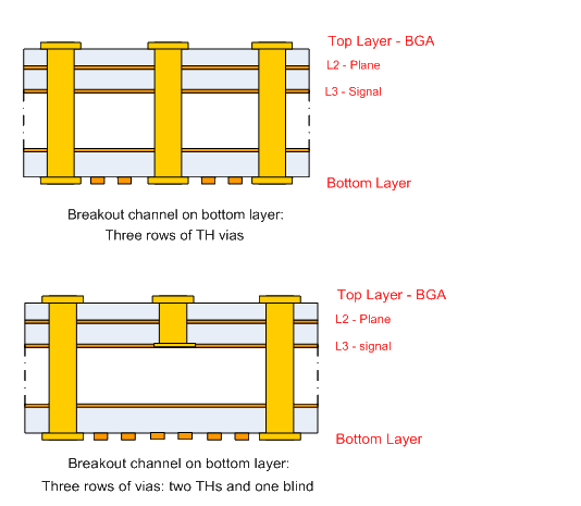
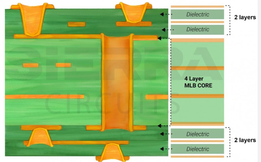
Via, also known as metalized holes, is one of the important components of PCB design. In double-sided and multi-layer boards, in order to connect the printed wires between the layers, a common hole, i.e., a via, is drilled at the intersection of the wires that need to be connected in each layer. Vias are divided into three categories, namely blind vias, buried vias, and through vias. This article collects some classic questions and answers about PCB “vias”, hoping to help everyone.
1.You often see a lot of holes on PCB boards. Are the more vias the better? Are there any rules?
Answer: No. Try to minimize the use of vias. When you have to use vias, you should also consider reducing the impact of vias on the circuit.
2.When laying out the board, if the lines are dense, there may be more vias, which will of course affect the electrical performance of the board. How can I improve the electrical performance of the board?
Answer: For low-frequency signals, vias don’t matter. For high-frequency signals, try to reduce vias. If there are many lines, you can consider multilayer boards.

3.How much influence do through holes and blind holes have on the difference of signals? What are the application principles?
Answer: Using blind or buried holes is an effective way to increase the density of multilayer boards, reduce the number of layers and board size, and greatly reduce the number of plated through holes. But in comparison, through holes are easy to implement in terms of process and have low cost, so through holes are generally used in designs.
4.Can you explain the proportional relationship between the line width and the size of the matching vias?
Answer: It is difficult to say that there is a simple proportional relationship because the two simulations are different. One is surface transmission and the other is ring transmission. You can find a via impedance calculation software on the Internet, and then keep the impedance of the via consistent with the impedance of the transmission line.
5.What is the relationship between the line width and the size of the via on the PCB board and the current passing through?
Answer: The copper foil thickness of a general PCB is 1 ounce, about 1.4 mil, and the maximum current allowed for a 1 mil line width is 1A. Vias are relatively complex. In addition to being related to the size of the via pad, they are also related to the thickness of the copper deposited on the hole wall after electroplating during the processing process.
6.Should the vias match the Sqrt (L/C) according to the needs?
Answer: Yes, simply put, it is impedance matching, and the parameters of the vias are adjusted to achieve a better impedance smooth transition.
7.Is there a corresponding relationship between temperature changes and the impedance of vias?
Answer: Temperature changes mainly affect the reliability of vias, and material selection requires consideration of the CTE value of the material.

8.For high-speed PCBs, how to avoid vias during wiring, what are some good suggestions?
Answer: For high-speed PCBs, it is best to make fewer vias and solve the need to increase vias by adding signal layers.
9.What is the role and principle of adding ground vias near routing vias?
A: The vias of PCB board can be classified into the following types according to their functions:
1) Signal vias (the via structure requires the minimum impact on the signal)
2) Power and ground vias (the via structure requires the via to have the minimum distributed inductance)
3) Heat dissipation vias (the via structure requires the via to have the minimum thermal resistance)
The vias mentioned above belong to the grounding type of vias. The function of adding grounding vias near the routing vias is to provide the shortest return path for the signal.
Note: The vias of signal layer change are a discontinuous point of impedance. The return path of the signal will be disconnected from here. In order to reduce the area surrounded by the return path of the signal, some ground vias must be drilled around the signal vias to provide the shortest signal return path and reduce the EMI radiation of the signal. This radiation will increase significantly with the increase of signal frequency.

10.In the case of a relatively small aperture of the signal via (such as 0.3mm diameter), will the via metallization be insufficient in this case?
A: If the aperture is small and deep (that is, the aperture is relatively large), it may not be fully metallized.


