Four Tips in PCB Design
It is said that every engineer has a lot of interesting experiences and unique technical experience in PCB design. I wonder what you think of the rules and experience of PCB design? Today, the editor has brought you a dry goods, which can teach you four tips in PCB design in ten minutes. Scroll down quickly~
This dry goods comes from Rob Reeder, a senior system application engineer in the industrial and instrumentation department of ADI, on the four important PCB layout and wiring rules for “using high-speed converters”. It is mainly to ensure that the design performance can meet the technical specifications of the data sheet, so designers must follow some basic guidelines.
1.Should the AGND and DGND ground planes be separated?
First, let’s solve a common problem, that is, “Should the AGND and DGND ground planes be separated?” The detailed answer is “usually not separated”. Because in most cases, separating the ground plane will only increase the inductance of the return current, so the disadvantages outweigh the benefits. From V=L(di/dt), it can be found that: as the inductance increases, the voltage noise will increase; and as the switching current increases, the voltage noise will also increase. Therefore, the ground planes should be tied together.
Splitting the ground planes is key to good performance in applications where traditional design requirements dictate that dirty bus power or digital circuits be placed in certain areas, and size constraints prevent good layout segmentation of the board. However, for the overall design to work, these ground planes must be tied together at a bridge or connection point somewhere on the board. Therefore, the connection points should be evenly distributed across the split ground planes. Eventually, there is often a connection point on the PCB that is the best place for return current to pass without degrading performance. This connection point is usually near or below the converter.
When designing the power planes, use all the copper available to these layers. If possible, do not share traces between these layers, as additional traces and vias can quickly degrade the power plane by breaking it up into smaller pieces. The resulting sparse power plane can squeeze current paths to where they are needed most, at the converter’s power pins. Squeezing current between vias and traces increases resistance, causing a slight voltage drop at the converter’s power pins.
Finally, the placement of the power plane is critical. Never stack a noisy digital power plane on an analog power plane. Otherwise, although the two are on different layers, they may still be coupled. To minimize the risk of system performance degradation, these types of layers should be separated as much as possible in the design instead of stacking them together.
2.Can the power delivery system design (PDS) of the PCB be ignored?
The design goal of the PDS is to minimize the voltage ripple generated in response to the power supply current demand. All circuits require current, some circuits require more, and some circuits need to provide current at a faster rate. The use of a well-decoupled low-impedance power or ground layer and a good PCB stackup can minimize the voltage ripple generated by the circuit’s current demand. For example, if the design has a switching current of 1A and the impedance of the PDS is 10mΩ, the maximum voltage ripple is 10mV.
First, a PCB stackup structure that supports large layer capacitance should be designed. For example, a six-layer stackup may include a top signal layer, a first ground layer, a first power layer, a second power layer, a second ground layer, and a bottom signal layer. The first ground plane and the first power plane are specified to be close to each other in the stackup, with a spacing of 2 to 3 mils between the two planes, creating an inherent layer capacitance. The best part about this capacitance is that it is free and only needs to be noted in the PCB manufacturing notes. If the power plane must be split, with multiple VDD rails on the same layer, use the largest possible power plane. Do not leave voids and be mindful of sensitive circuits. This will maximize the capacitance of that VDD plane. If the design allows for additional layers (in this case, going from six to eight), two additional ground planes should be placed between the first and second power planes. With the same 2 to 3 mil core spacing, the inherent capacitance of the stackup will now double.
For an ideal PCB stackup, decoupling capacitors should be used at the entry point of the power plane and around the DUT, which will ensure that the PDS impedance is low over the entire frequency range. Using several 0.001μF to 100μF capacitors helps cover this range. It is not necessary to have capacitors everywhere; having capacitors butted right up against the DUT will break all manufacturing rules. If such drastic measures are required, there is something else wrong with the circuit.
3.How to use the exposed pad to achieve the best PCB connection?
(1)Exposed pad
The exposed pad is very important for the full performance of the signal chain and the adequate heat dissipation of the device. The exposed pad, which ADI calls Pin 0, is the pad under most devices today. It is an important connection through which all the internal grounds of the chip are connected to the center point under the device. I wonder if you have noticed that many converters and amplifiers today lack a ground pin, and the reason is the exposed pad.
Properly fixing (i.e. soldering) this pin to the PCB can achieve a reliable electrical and thermal connection. If this connection is not strong, it will be a mess; in other words, this design is likely to become an invalid design that the designer does not want to see.
(2)How to achieve the best connection
There are three steps to achieve the best electrical and thermal connection using the exposed pad-
- When possible, the exposed pad should be replicated on each PCB layer. The purpose of this is to form a dense thermal connection with all grounds and ground planes, thereby quickly dissipating heat. This step is related to high-power devices and applications with high channel counts. Electrically, this will provide a good equipotential connection for all ground planes. You can even replicate the exposed pad on the bottom layer (see Figure 1), which can be used as a decoupling thermal ground point and a place to mount a bottom-side heat sink.

Exposed pad layout example
- Split the exposed pad into multiple identical sections, like a chessboard. Use a silk screen cross grid on the exposed pad that is open, or use a solder mask. This step ensures a solid connection between the device and the PCB. During the reflow assembly process, there is no way to determine how the solder paste will flow and ultimately connect the device to the PCB. The connection may exist, but it is unevenly distributed. You may only get one connection, and it is small, or worse, located in a corner. Splitting the exposed pad into smaller sections ensures that each area has a connection point, resulting in a more secure and evenly connected exposed pad (see Figures 2 and 3).
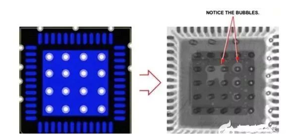
Example of improper EPAD layout
Example of better EPAD layout
- You should ensure that each section has a via connected to the ground. The area is usually large enough to place multiple vias. Before assembly, it is important to fill each via with solder paste or epoxy. This step is very important to ensure that the exposed pad solder paste does not flow back into these via voids and prevent proper connection.
4.Is cross-coupling between PCB layers really irrelevant?
In PCB design, the layout and routing of some high-speed converters will inevitably overlap one circuit layer with another. In some cases, sensitive analog layers (power, ground, or signal) may be right above a noisy digital layer. Because these layers are on different layers, it doesn’t matter? Let’s look at a simple test.
Select one of the adjacent layers and inject a signal on this layer. Then connect the cross-coupled layer to a spectrum analyzer. You can see that there is a lot of signal coupling to the adjacent layer. Even with a spacing of 40 mils, the adjacent layers still form a capacitor in a sense, so at some frequencies, the signal will still couple from one layer to another.
Assume a noisy digital section on one layer has a 1V signal switching at high speed. With 60dB isolation between layers, the non-driven layer will see a 1mV signal coupled from the driven layer. For a 12-bit analog-to-digital converter (ADC) with a 2Vp-p full-scale swing, this means a coupling of 2LSBs (least significant bits). This may not be a problem for a particular system, but be aware that when the resolution increases from 12 to 14 bits, the sensitivity increases by a factor of four, increasing the error to 8LSBs.
Ignoring cross-plane/cross-layer coupling may not cause a system design to fail or compromise, but it is important to be vigilant because there may be more coupling between two planes than you think.
Be aware of this when you see noise spurious coupling within the spectrum of interest. Sometimes layout and routing can cause unexpected signals or layers to cross-couple to different layers. Keep this in mind when debugging sensitive systems: the problem may be in the layer below