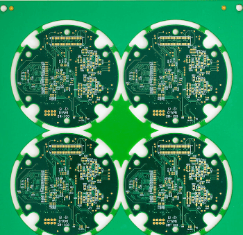
Teach You Six Troubleshooting Problems Related to High-speed PCBs
During PCB design,we often encounter various issues,such as impedance matching and EMI regulations.This article summarizes some high-speed PCB-related FAQ,hoping to be helpful.
1.How to Consider Impedance Matching When Designing High-speed PCB Schematics?
Impedance matching is a key design factor in high-speed PCB circuit design.Impedance values are closely related to the routing method.such as whether the trace is routed on a surface layer(microstrip) or an inner layer(stripline/double stripline),the distance from the reference layer(power or ground layer),the trace width,and the PCB material,all of which affect the trace’s characteristic impedance.
This means that impedance values can only be determined after routing.Due to limitations in the circuit model or the mathematical algorithms used,typical simulation software cannot account for routing situations with impedance discontinuities.In these cases,terminators(such as series resistors) can be used on the schematic to mitigate the effects of trace impedance discontinuities,The true solution is to minimize impedance discontinuities during routing.
2.When a PCB contains multiple digital/analog functional blocks.It is common practice to separate the digital and analog ground planes.why?
Separate digital/analong ground planes are necessary because digital circuits generate noise in the power supply and ground planes when switching between high and low voltages.The amount of noise depends on the signal speed and current
If the ground plane is not separated and the noise generated by the digital circuits is high while the analog circuits are very close together,even if the digital and analog signals don’t cross,the analog signals will still be affected by the ground noise.In other words,unseparated digital and analog ground planes should only be used when the analog circuits are far away from the noise-generating digital circuits.

3.When designing high-speed PCBs,what aspects of EMC and EMI should designers consider?
Generally,EMI/EMC design requires consideration of both radiated and conducted emissions.The radiated emissions relate to higher frequencies(>30 MHz),while the conducted emission relate to lower frequencies(<30 MHz).Therefore, one shouldn’t focus solely on high frequencies while ignoring low frequencies.
A good EMI/EMC design must consider component placement,PCB stackup arrangement,critical connection routing,and component selection from the very begining.Without optimal planning upfront,addressing these issues later will result in ineffective result and increased costs.
For example,the clock generator should be positioned as close to external connectors as possible.High-speed signals should be routed on inner layers,ensuring impedance matching and reference layer continuity to minimize reflections.The slew rate of the signals driven by the components should be minimized to reduce high-frequency component.When selecting decoupling (bypass) capacitors,consider whether their frequency response meet requirements to reduce power plane noise.
In addition,the return path of high-frequency signal current should be kept as small as possible(i.e., loop impedance) to minimize radiation. Ground planes can also be split to control the range of high-frequency noise. Finally, the ground points between the PCB and chassis should be appropriately selected.
4.When designing the PCB, should the ground trace be closed to minimize interference?
When designing the PCB, it is generally necessary to minimize loop area to reduce interference. When laying ground traces, they shouldn’t be laid in a closed pattern; instead, a dendritic pattern is preferred. Also, the ground area should be maximized.
5.How can I adjust the routing topology to improve signal integrity?
Signal directions in this type of network are complex. Because topology affects unidirectional and bidirectional signals, as well as signals of different levels and types, differently, it’s difficult to determine which topology is best for signal quality. Furthermore, determining the right topology during pre-simulation requires a high level of understanding of circuit principles, signal types, and even routing difficulty.
6.How can I ensure the stability of signals over 100 Mbps during layout and routing?
The key to high-speed digital signal routing is minimizing the impact of transmission lines on signal quality. Therefore, when laying out high-speed signals over 100 Mbps, signal traces must be kept as short as possible. In digital circuits, high-speed signals are defined by their rise time.
Furthermore, different signal types (such as TTL, GTL, and LVTTL) require different methods for ensuring signal quality.


