
PCB Tooling Holes: Size and Placement for Manufacturing
Every fabrication line relies on tooling holes to register panels across drilling, imaging, and lamination. A 0.1mm registration error on a 16-layer board propagates through each lamination cycle, producing misaligned vias and torn annular rings by final electrical test. Tooling holes anchor your design to physical reality—when sized and placed correctly, they deliver sub-0.05mm layer-to-layer registration. Specify them wrong, and even perfect Gerber files yield scrap.
What Are PCB Tooling Holes?
Tooling holes are non-plated through-holes drilled into PCB panels to provide mechanical reference points during fabrication and assembly. Unlike mounting holes that secure the finished board, tooling holes exist solely to align panels on manufacturing equipment.
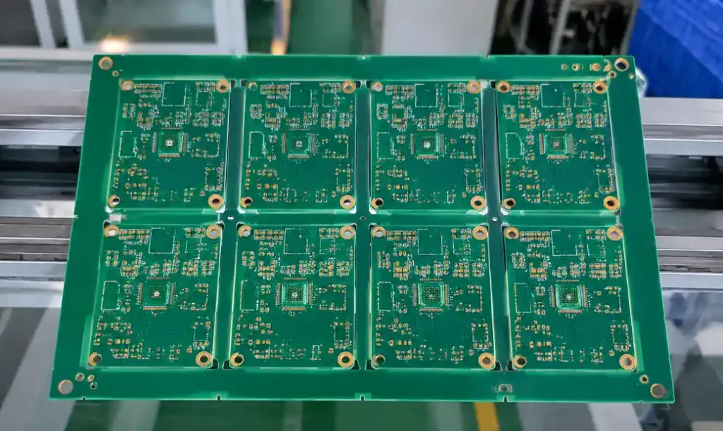
Fabricators use tooling holes to register each layer during drilling, maintain alignment through lamination, and position panels on SMT fixtures. The holes typically remain in breakaway rails or panel corners, removed during depanelization.
According to IPC-6012D, tooling holes must maintain ±0.075mm positional tolerance for Class 2 products and ±0.05mm for Class 3 high-reliability applications. These tolerances directly affect layer registration and via-to-pad alignment across the panel.
Standard Tooling Hole Sizes
Manufacturing equipment worldwide standardizes on three tooling hole diameters: 2.0mm, 2.4mm, and 3.0mm. Equipment manufacturers design registration pins, drill spindles, and SMT fixture locators around these sizes.
| Hole Size | Primary Application | Registration Accuracy | Typical Use Case |
|---|---|---|---|
| 2.0mm | Laser drilling registration, fine-pitch SMT | ±0.03mm | HDI boards, 0201 components, >0.4mm pad pitch |
| 2.4mm | Standard SMT assembly, testing fixtures | ±0.05mm | General production, 0402-0603 components |
| 3.0mm | Panel handling, wave soldering | ±0.08mm | Large panels, through-hole assembly, heavy boards |
The 2.4mm hole dominates SMT assembly lines because pick-and-place machines from Panasonic, Juki, and Fuji ship with 2.4mm locating pins as standard. Going smaller than 2.0mm risks pin breakage; going larger than 3.0mm weakens panel edges.
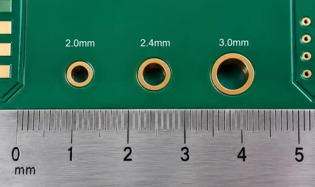
For HDI multilayer designs with microvias, specify 2.0mm tooling holes. The tighter pin fit reduces play during layer registration, critical when drilling 0.15mm laser vias that must hit 0.3mm capture pads across multiple lamination cycles.
Tooling Hole Placement for Panel Registration
Placement strategy directly controls registration accuracy. Tooling holes must form a rigid geometric constraint system that eliminates panel rotation and translation errors.
The standard configuration uses three holes in a non-collinear pattern. Two holes along one axis define X-Y position and rotation; the third hole, offset perpendicular, constrains the second rotational degree. This three-point kinematic mount achieves deterministic positioning.
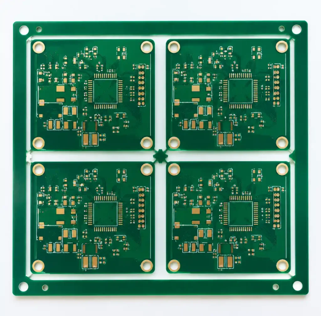
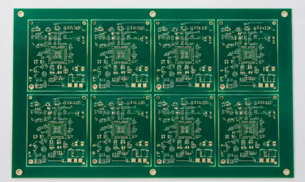
Place tooling holes in panel corners or breakaway rails, never within the active board area. Minimum edge distance is 5mm to prevent drill breakout. For panels larger than 400×500mm, add a fourth hole at center to control flexural deflection during lamination.
Hole spacing matters as much as count. Tooling holes separated by less than 100mm cannot adequately constrain a 250×300mm panel. Aim for maximum diagonal spacing, typically placing holes at opposite corners with a third hole midway along one edge.
Tooling Holes for SMT Assembly
SMT equipment demands different tooling strategies. Assembly fixtures clamp panels using the same tooling holes, but also require fiducials for optical alignment. Separate the functions—tooling holes provide coarse mechanical positioning (±0.1mm), while fiducials give vision systems fine alignment (±0.01mm).
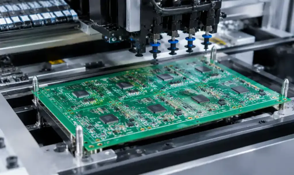
For panelized designs, add tooling holes to the panel frame, not individual boards. Breaking apart boards before assembly loses the reference frame. If assembling individual boards, include two tooling holes per board positioned diagonally.
Component density affects placement. Panels with 0201 passives or 0.4mm pitch BGAs require 2.0mm tooling holes minimizing distance from holes to components. Pick-and-place positional error grows with distance from the reference. Keep critical components within 150mm of the nearest tooling hole cluster.
Non-Plated vs Plated Tooling Holes
Non-plated tooling holes are standard for registration. They maintain precise diameter through fabrication because no copper deposition occurs. Drill a 2.4mm hole, and you get 2.40mm ±0.05mm finished—exactly what registration pins expect.
Plating adds 25-40µm copper per side, shrinking a 2.4mm drilled hole to 2.32-2.35mm. This creates clearance problems with standard pins. Plating thickness also varies with panel position—edge holes plate thinner than center holes. A 30µm variation translates to 0.03mm registration error.
| Hole Type | Diameter Consistency | Registration Accuracy | When to Use |
|---|---|---|---|
| Non-Plated | ±0.03mm across panel | ±0.03-0.05mm | Standard fabrication, SMT assembly, precision work |
| Plated | ±0.08mm across panel | ±0.08-0.12mm | When hole must double as grounded mount point |
Use plated tooling holes only when the hole serves dual function—registration during assembly and grounded mounting on the finished product. Better practice: use non-plated 2.4mm tooling holes for manufacturing, plus separate 3.0mm plated mounting holes offset 5mm away.
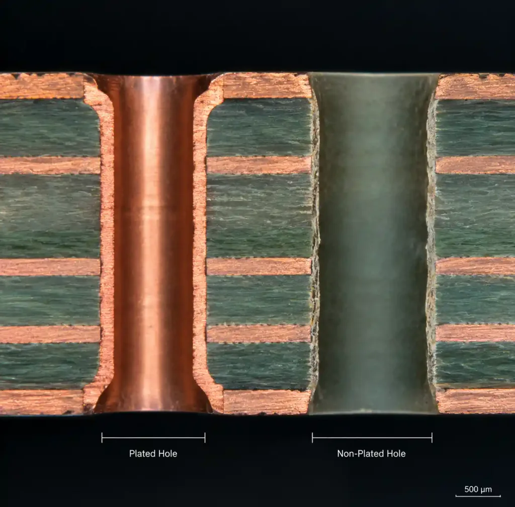
For multilayer HDI boards requiring 0.05mm alignment, specify non-plated tooling holes explicitly in fabrication drawings. Add a note: “Tooling holes to remain non-plated through all processes.”
Tooling Hole Spacing and Board Thickness
Board thickness changes how tooling holes interact with registration pins. Thin boards (0.4-0.8mm) flex during handling, requiring more tooling holes to constrain movement. Thick boards (2.4-3.2mm) need larger holes—a 3.2mm board with 2.0mm holes risks drill wander.
For flexible circuits, tooling holes must penetrate the rigid support carrier, not the flex layer. Drilling the flex creates stress points that propagate into cracks.
Panel size scales tooling hole requirements. A 200×250mm panel needs three holes minimum. A 500×600mm panel needs six to eight holes to control mid-panel sag.
Tooling Holes and Testing Fixtures
Electrical test fixtures—flying probe testers, ICT beds, and functional test jigs—rely on tooling holes for board positioning. Flying probe systems use two tooling holes for coarse alignment, then optically locate test points. ICT fixtures require tighter control because spring-loaded pins must hit pads without visual feedback.
Use 2.0mm tooling holes with ±0.03mm positional tolerance for ICT, enabling 0.5mm test pads with consistent contact. Coordinate tooling hole locations across design, fabrication, assembly, and test to eliminate re-registration errors.
Registration Accuracy and Tolerances
Registration accuracy determines how well layers align during fabrication and how precisely machines position panels. Poor registration manifests as misaligned vias, broken connections, and soldermask-to-pad misregistration.
IPC-6012 defines three classes. Class 1 allows ±0.13mm layer-to-layer. Class 2 tightens to ±0.075mm. Class 3 demands ±0.05mm. Medical devices, aerospace, and automotive ADAS systems fall under Class 3.
Tooling hole position tolerance contributes directly to these targets. A ±0.05mm hole position error consumes the entire Class 3 budget. Realistic tolerance stacking:
- Tooling hole drilling: ±0.03mm
- Layer imaging to holes: ±0.02mm
- Lamination shift: ±0.02mm
- Final drill to layer: ±0.03mm
Total registration error: ±0.10mm (2σ), exceeding Class 3 limits. This is why 50-layer boards with sequential lamination need 2.0mm tooling holes re-drilled after each cycle.
Common Tooling Hole Mistakes
Placing tooling holes inside the board outline forces them into the active circuit area, wasting routing space and creating clearance conflicts. Always locate tooling holes in panel rails or breakaway tabs.
Specifying only two tooling holes fails to constrain panel rotation. The board can spin around the two-hole axis, producing registration errors. Always use minimum three holes in a non-collinear pattern.
Using different hole sizes across a panel breaks equipment compatibility. Pick-and-place machines expect uniform tooling pins—mixing 2.4mm and 3.0mm holes requires manual intervention to swap pins.
Failing to specify non-plated creates ambiguity. Many fabricators plate all holes by default unless explicitly told otherwise. Your fabrication drawing must state: “Holes X1, X2, X3 to remain non-plated through all processes.”
Ignoring hole-to-copper clearance around tooling holes creates shorts when the panel shifts. Maintain 1.5mm minimum clearance between the tooling hole edge and any copper feature.
Tooling Holes in Design Files
Gerber files must explicitly identify tooling holes so CAM engineers recognize them as non-functional features. In your drill file, create a separate layer or symbol for tooling holes distinct from vias and mounting holes.
Most CAM software expects tooling holes marked with a unique aperture code or placed on a dedicated mechanical layer. Include a fabrication note: “Holes marked TH1, TH2, TH3 are non-plated tooling holes, 2.4mm finished diameter, ±0.05mm positional tolerance.”
For panelized production, coordinate tooling hole locations with your fabricator before finalizing the design. They can provide panel templates showing optimal hole positions for their equipment.
Export tooling hole coordinates in a separate file (CSV or text) alongside Gerbers. Include X-Y position, diameter, and plating status for each hole. This redundancy prevents misinterpretation.
FAQ
What size should PCB tooling holes be?
Standard sizes are 2.0mm, 2.4mm, and 3.0mm. Use 2.4mm for general SMT assembly—it matches industry-standard fixture pins. Use 2.0mm for HDI boards requiring ±0.03mm registration accuracy. Use 3.0mm only for large panels (>500×600mm) or thick boards (>2.4mm).
How many tooling holes does a PCB panel need?
Minimum three holes in a non-collinear pattern—typically two holes along one edge and a third offset perpendicular. Panels larger than 400×500mm need four to six holes to control mid-panel flexure.
Should tooling holes be plated or non-plated?
Non-plated for precision work. Plating shrinks hole diameter by 0.05-0.08mm, creating loose fits on registration pins and introducing ±0.03-0.05mm positional error. Use plated tooling holes only when the same hole must serve as a grounded mounting point—and even then, consider using separate holes.
Where should I place tooling holes on my PCB?
In panel corners or along breakaway rails, never inside the active board area. Maintain 5mm minimum edge distance to prevent drill breakout. Maximize diagonal spacing between holes—place them at opposite panel corners with a third hole midway along one edge.
Do tooling holes need soldermask clearance?
Yes. Even though tooling holes are non-plated, they need soldermask clearance to prevent process contamination. Specify 0.3-0.5mm soldermask expansion around each tooling hole. This keeps solder mask from wicking into the hole and ensures clean pin insertion.
Conclusion
Tooling holes are the mechanical foundation of PCB manufacturing accuracy. Correct sizing (2.4mm standard, 2.0mm for HDI) and placement (three-hole non-collinear minimum) directly control registration errors across drilling, lamination, assembly, and test. Keep holes non-plated, maintain ±0.05mm positional tolerance for Class 3 work, and place them in panel corners or breakaway rails with maximum diagonal spacing.
Coordinate tooling hole positions with your fabricator early in the design phase. For high-layer-count boards, plan for tooling hole re-drilling after each lamination cycle to prevent tolerance accumulation. Mark tooling holes explicitly in your Gerber files and export coordinates separately to avoid CAM misinterpretation.
Andwin Circuits specializes in precision Class 3 PCB manufacturing with sub-0.05mm registration accuracy. Our engineering team reviews tooling hole placement during DFM analysis to ensure your design meets production requirements. Contact us for tooling optimization guidance on your next project.