
PCB Copper Weight Selection: 1oz vs 2oz vs 3oz for Different Applications
Current-carrying failures account for 25-35% of PCB-related field returns in power electronics and automotive sectors. The root cause? Undersized copper that cannot handle peak loads or thermal stress. Selecting proper copper weight from the start saves months of rework and eliminates costly field failures.
What is PCB Copper Weight?
Copper weight measures the mass of copper per square foot, expressed in ounces (oz/ft²). This directly correlates to thickness: 1 oz equals 35 μm (1.4 mils), 2 oz equals 70 μm (2.8 mils), and 3 oz equals 105 μm (4.2 mils). Standard boards use 1 oz copper for inner and outer layers, but applications above 3-5A per trace require thicker copper to prevent resistive heating and voltage drops.
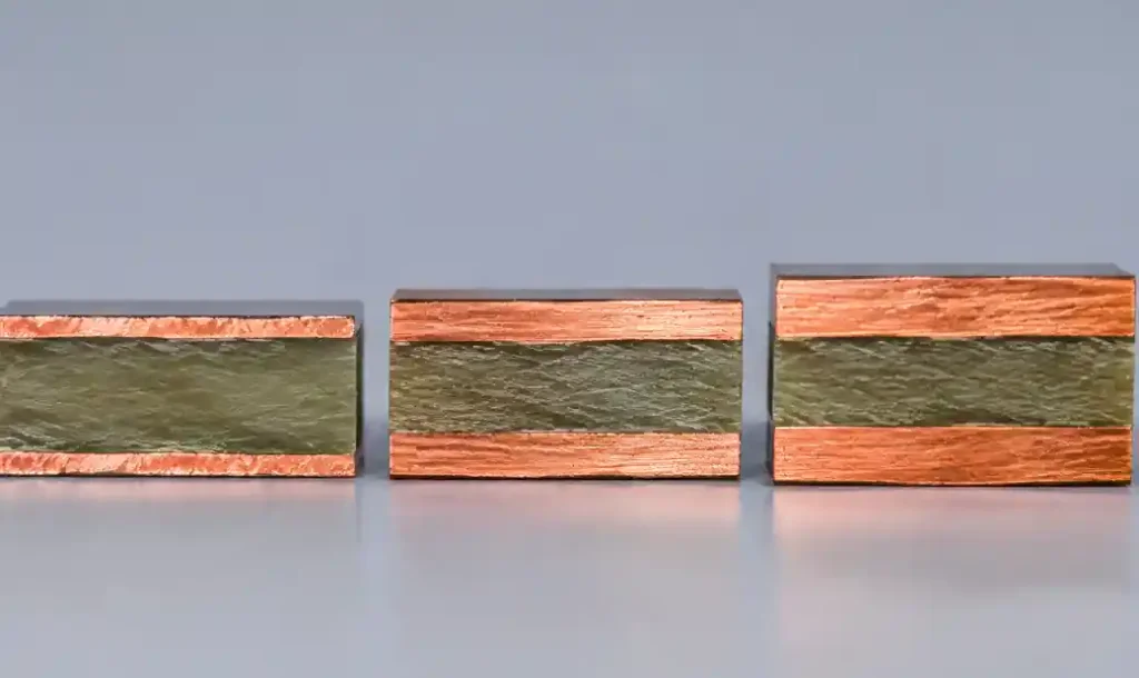
IPC-2152 supersedes the older IPC-2221 charts, providing more accurate current capacity data based on extensive empirical testing. The standard accounts for trace geometry, copper thickness, ambient temperature, and board construction—internal vs external layers matter significantly since internal traces dissipate heat less effectively.
Current Carrying Capacity by Copper Weight
Temperature rise directly affects reliability. Each 10°C increase above rated operating temperature roughly halves semiconductor lifespan per Arrhenius equation. Conservative designs target 10°C rise for consumer products, 5°C for automotive and industrial applications operating at high ambient temperatures.
| Copper Weight | 5A (10°C rise) | 10A (10°C rise) | 15A (10°C rise) | 20A (10°C rise) |
|---|---|---|---|---|
| 1 oz (35 μm) | 90 mils (2.3 mm) | 181 mils (4.6 mm) | 272 mils (6.9 mm) | 362 mils (9.2 mm) |
| 2 oz (70 μm) | 45 mils (1.1 mm) | 90 mils (2.3 mm) | 136 mils (3.5 mm) | 181 mils (4.6 mm) |
| 3 oz (105 μm) | 30 mils (0.76 mm) | 60 mils (1.5 mm) | 90 mils (2.3 mm) | 121 mils (3.1 mm) |
For a 10A trace with 10°C rise, 2 oz copper requires only 90 mils width versus 181 mils with 1 oz—a 50% reduction enabling denser layouts. This becomes critical in space-constrained designs like HDI PCBs where routing channels are limited.
Power dissipation follows P = I² × R. A 100 mm trace carrying 10A in 1 oz copper (2.3 mm wide) has ~1.1 mΩ resistance, dissipating 110 mW as heat. The same trace in 2 oz copper drops to 0.55 mΩ and 55 mW—cutting losses by 50%. This matters in battery-powered devices where every milliwatt counts.
1oz Copper: Applications and Limitations
Standard 1 oz copper dominates consumer electronics, IoT devices, and signal-processing boards. Manufacturing cost is lowest, etching achieves 3-4 mil trace/space capability, and most fabs stock 1 oz foil reducing lead time. Use 1 oz when current remains below 3-5A per trace and operating temperature stays under 70°C ambient.
Typical applications: Smartphones, routers, USB peripherals, audio amplifiers under 20W, LED drivers below 500 mA per channel, PCB assembly for consumer products.
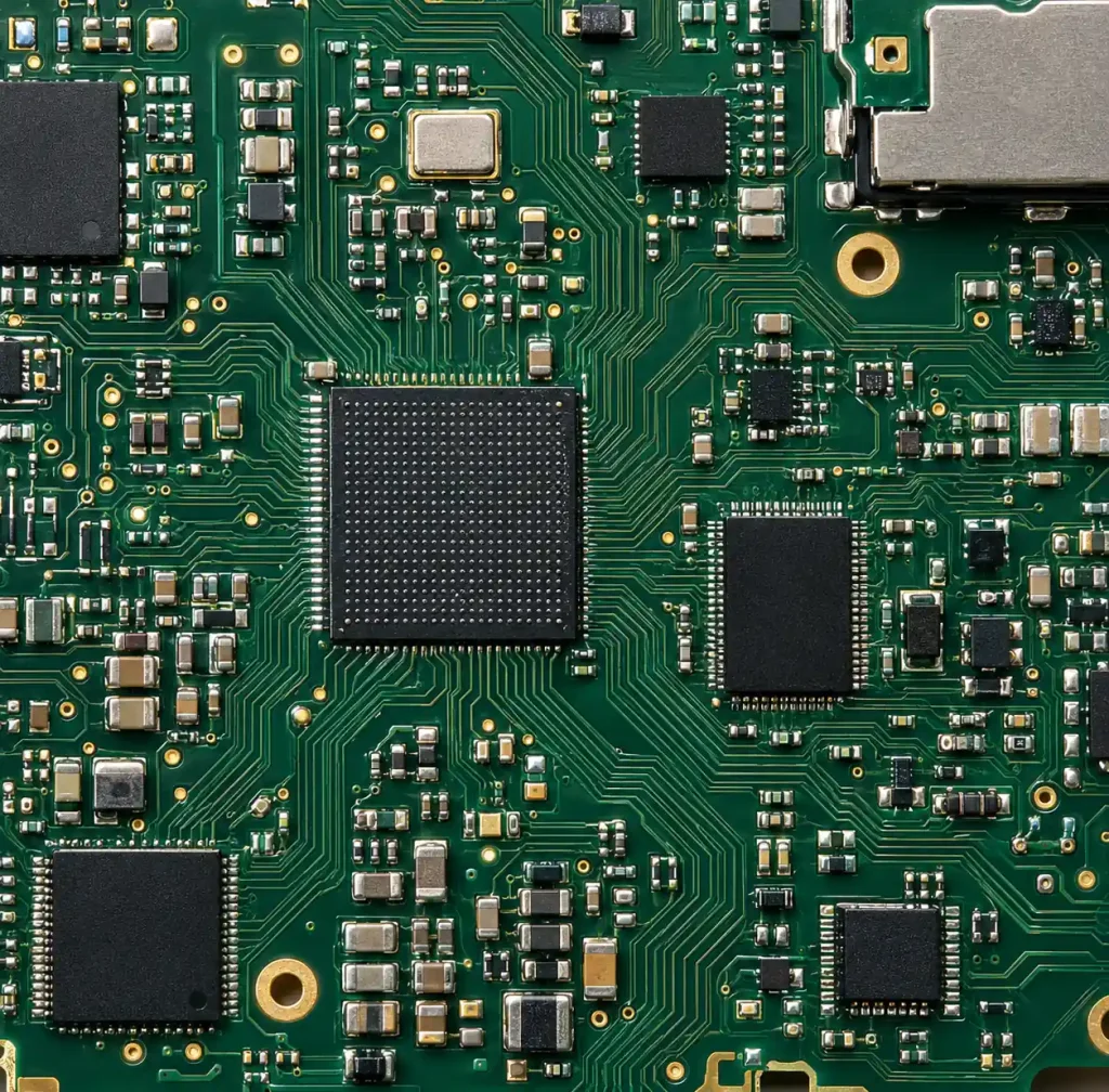
Limitations appear in high-current paths. A 15A trace requires 272 mils (6.9 mm) width—consuming significant board area. Voltage drops also increase: 100 mm at 15A drops 16.5 mV with 1 oz copper versus 8.3 mV with 2 oz.
Fine-pitch components (0.4 mm BGA, 0201 passives) benefit from 1 oz copper’s superior etching precision. Thicker copper creates undercutting during etching—for 3 oz copper, expect 3-4 mils undercut per side.
2oz Copper: The Balanced Choice
I specify 2 oz copper for 75% of power electronics designs—it hits the sweet spot between current capacity, cost, and manufacturability. Most PCB fabs handle 2 oz copper as a standard process with 5-7 mil trace/space capability, adding only 15-25% to 1 oz copper pricing.
Optimal applications: Motor controllers (up to 3 kW), battery management systems (10-30A charge/discharge), DC-DC converters (5-15A output), LED power supplies (1-3A channels), automotive body electronics.
| Current | 1 oz Width | 2 oz Width | Board Space Saved |
|---|---|---|---|
| 5A | 90 mils (2.3 mm) | 45 mils (1.1 mm) | 50% |
| 10A | 181 mils (4.6 mm) | 90 mils (2.3 mm) | 50% |
| 15A | 272 mils (6.9 mm) | 136 mils (3.5 mm) | 50% |
Resistance drops by half versus 1 oz copper, which matters in applications where efficiency determines battery life. A 5 kW motor controller dissipates 150-200W in copper losses with 1 oz copper on power traces, versus 75-100W with 2 oz.
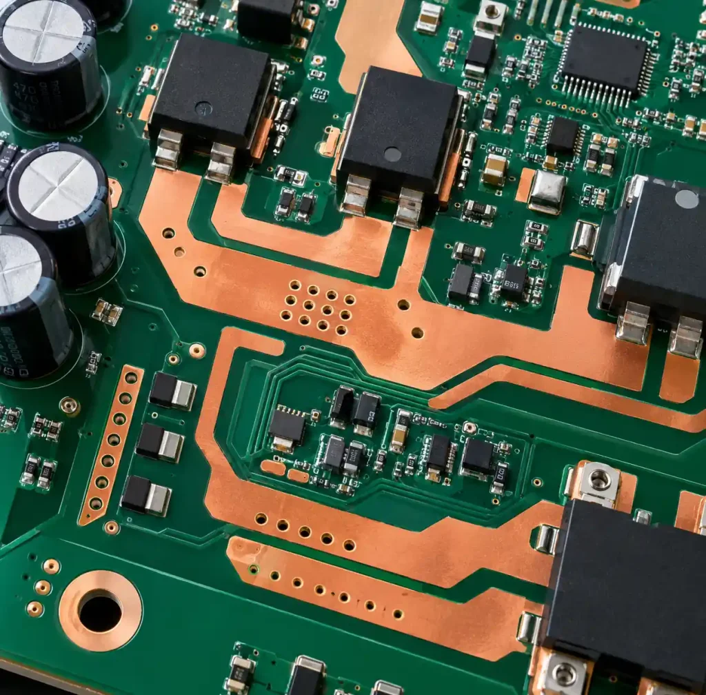
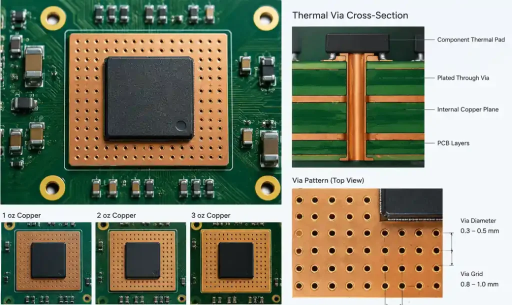
Design considerations: Via current ratings scale with barrel area, so use multiple parallel vias for layer transitions. Four 12-mil vias handle 10-12A where a single via manages only 2.5-3A. Thermal vias spaced 0.5-0.8 mm improve heat spreading to internal planes.
3oz Copper and Heavy Copper: When Standard Isn’t Enough
3 oz copper enters when current exceeds 20A per trace or operating temperature approaches 100°C. I’ve used 3-6 oz copper in EV charging stations, industrial welding equipment, high-power LED arrays above 500W, and three-phase motor drives. The 40-60% price premium over 2 oz copper pays off by eliminating thermal management issues.
Prime applications: EV onboard chargers (7-22 kW), DC fast charging stations (50-350 kW), industrial inverters (5-50 kW), photovoltaic inverters, induction heating, heavy copper PCB for power modules above 1 kW continuous.
Manufacturing impacts design rules. Minimum trace/space increases to 10-12 mils for 3 oz copper due to etching undercutting. Annular rings must grow to 8-10 mils to prevent breakout during drilling. Aspect ratio (board thickness / hole diameter) limits tighten—keep ratios below 6:1 for reliable plating in thick copper.
Copper balancing becomes critical with heavy copper. Solid pours on power layers create warpage during lamination unless balanced by hatched copper on signal layers. Target 30-50% copper coverage per layer to prevent 0.5-2 mm bow across 200 mm boards, which causes assembly yield loss.
Thermal Performance Comparison
Copper thickness directly affects thermal conductivity through the board. While FR4’s 0.3 W/m·K limits through-thickness heat flow, copper’s 385 W/m·K enables lateral heat spreading. Thicker copper reduces thermal resistance from hot spots to surrounding planes by increasing conductive cross-section.
| Configuration | Thermal Resistance (°C/W) | Temperature Rise at 5W |
|---|---|---|
| 1 oz copper, no thermal vias | 12-15 | 60-75°C |
| 2 oz copper, no thermal vias | 8-10 | 40-50°C |
| 2 oz copper, via array | 5-6 | 25-30°C |
| 3 oz copper, via array | 3-4 | 15-20°C |
For components dissipating 3-10W (power MOSFETs, LDOs, high-current drivers), thermal via arrays connecting to internal planes dramatically lower junction temperature. Combine 2 oz copper with 0.3-0.5 mm thermal vias on 1 mm grid—this often eliminates the need for metal core PCB in moderate-power designs.
Cost and Lead Time Analysis
Copper weight directly impacts PCB cost and availability. Standard 1 oz copper ships in 5-7 days from most fabs with $50-150 pricing for 4-layer prototypes. 2 oz copper adds 15-25% cost with similar lead times.
3 oz copper increases cost 40-60% and extends lead time to 10-15 days. Heavy copper above 4 oz requires specialized equipment, pushing lead time to 15-20 days. Design trade-offs matter: can you use 2 oz copper with wider traces instead of 3 oz with tighter routing?
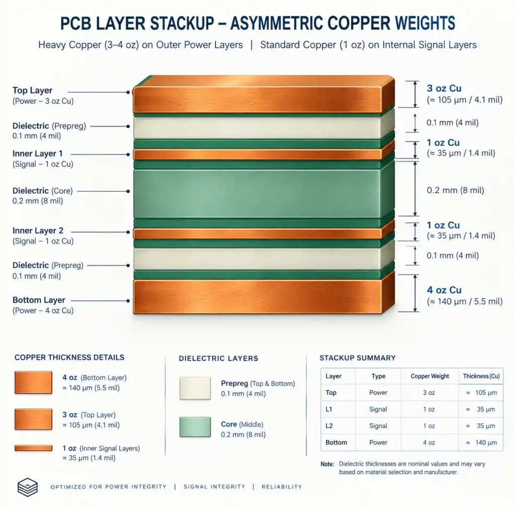
Cost optimization: Use mixed copper weights—specify heavy copper only on high-current layers (power planes, motor phases) while keeping signal layers at 1 oz. Many fabs support asymmetric copper at modest upcharges.
Design Rules by Copper Weight
Manufacturing capabilities constrain minimum feature sizes. Standard design rules adjust based on copper thickness:
1 oz copper: 3-4 mil trace/space (prototype), 5-6 mil (production), 5 mil minimum via annular ring, supports microvias down to 4 mil diameter.
2 oz copper: 5-6 mil trace/space (prototype), 7-8 mil (production), 6 mil minimum annular ring, etching undercut approximately 1.5-2 mils per side.
3 oz copper: 10-12 mil trace/space minimum, 8-10 mil annular ring, etching undercut 3-4 mils per side, avoid fine-pitch BGAs below 0.5 mm pitch.
Corner geometry affects current density. Sharp 90° corners concentrate current, causing hot spots. Use 45° chamfers or radiused corners with radius ≥ 2× trace width to reduce current crowding by 30-40%.
Selecting Copper Weight for Your Application
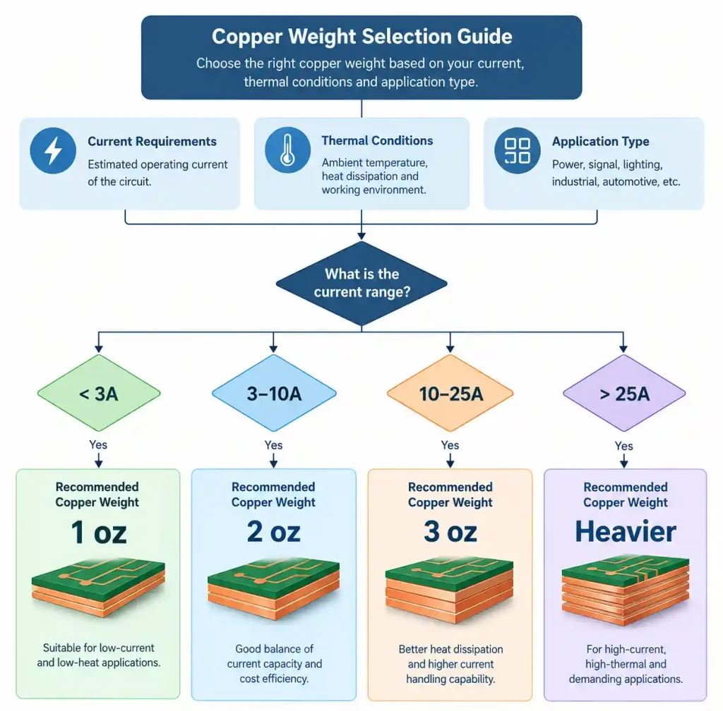
Start with current requirements. Calculate maximum continuous current per trace using IPC-2152 charts—add 20-30% safety margin for peak transients.
Decision framework:
< 3A per trace: 1 oz copper sufficient unless extreme space constraints or efficiency requirements push toward 2 oz.
3-10A per trace: 2 oz copper provides best balance—compact routing, good efficiency, standard manufacturing.
10-25A per trace: 2-3 oz copper required depending on thermal environment. Use 3 oz in high ambient temperature (>70°C) or where forced cooling isn’t practical.
> 25A per trace: 3 oz minimum, likely 4-6 oz for currents above 40-50A. Thermal analysis becomes mandatory.
Account for ambient temperature—a design operating at 85°C ambient allows less temperature rise than one at 25°C. Derating curves in IPC-2152 show capacity reductions: at 100°C ambient, current capacity drops 40-50% compared to 25°C baseline. This matters for automotive PCB and industrial applications.
FAQ
Can I mix copper weights on different layers?
Yes, asymmetric copper stackups use heavy copper on power layers with standard copper on signal layers. Specify this clearly in fabrication drawings since it affects impedance calculations.
How do I calculate via current rating?
A 12 mil via with 1 oz plating through 1.6 mm board handles approximately 2.5-3A with 10°C rise. Use multiple parallel vias for higher current—four vias provide roughly 4× capacity. IPC-2152 Appendix A contains detailed charts.
Does copper weight affect impedance?
Yes, thicker copper increases effective trace width due to copper sidewall angle, lowering characteristic impedance by 5-10% when going from 1 oz to 2 oz. Recalculate controlled impedance traces using your fab’s stackup parameters.
What about copper weight in flex PCB?
Flexible circuits typically use 0.5 oz or 1 oz copper to maintain flexibility. 2 oz copper in flex reduces bend cycles from 100,000+ to 10,000-50,000.
How does heavy copper impact assembly?
Thicker copper increases thermal mass, requiring higher reflow temperatures. Adjust reflow profiles—increase preheat temperature by 5-10°C per ounce above standard. Solder mask registration tolerances tighten, requiring 3-4 mil additional clearance for 3 oz copper.
Conclusion
Copper weight selection fundamentally impacts PCB performance, reliability, and cost. 1 oz copper serves signal-level and low-power designs where current stays below 3-5A. 2 oz copper handles 75% of power electronics applications with currents up to 15-20A. 3 oz and heavier copper become necessary above 20-25A or in thermally demanding environments. The decision involves trade-offs between board area, efficiency, cost, and lead time. Running IPC-2152 calculations early prevents undersized traces that fail in the field. For mission-critical applications, thermal simulation validates calculations before fabrication, saving weeks of troubleshooting and redesign cycles.