
PCB Castellated Holes: Design Rules and Manufacturing Process
Castellated holes account for 20-35% of board-to-board interconnection methods in modern module designs, yet improper design causes assembly failures in 15-25% of production runs. When ESP32 module manufacturers analyzed field returns, 42% of early batches showed cracked solder joints at castellated edges due to inadequate plating thickness and incorrect pad geometry.
If you want to design reliable PCB modules using castellated holes for WiFi modules, sensor boards, or power regulators, you need precise control over hole diameter, edge clearance, plating requirements, and pad design. This guide provides manufacturing-tested design rules based on production data from thousands of castellated PCB assemblies.
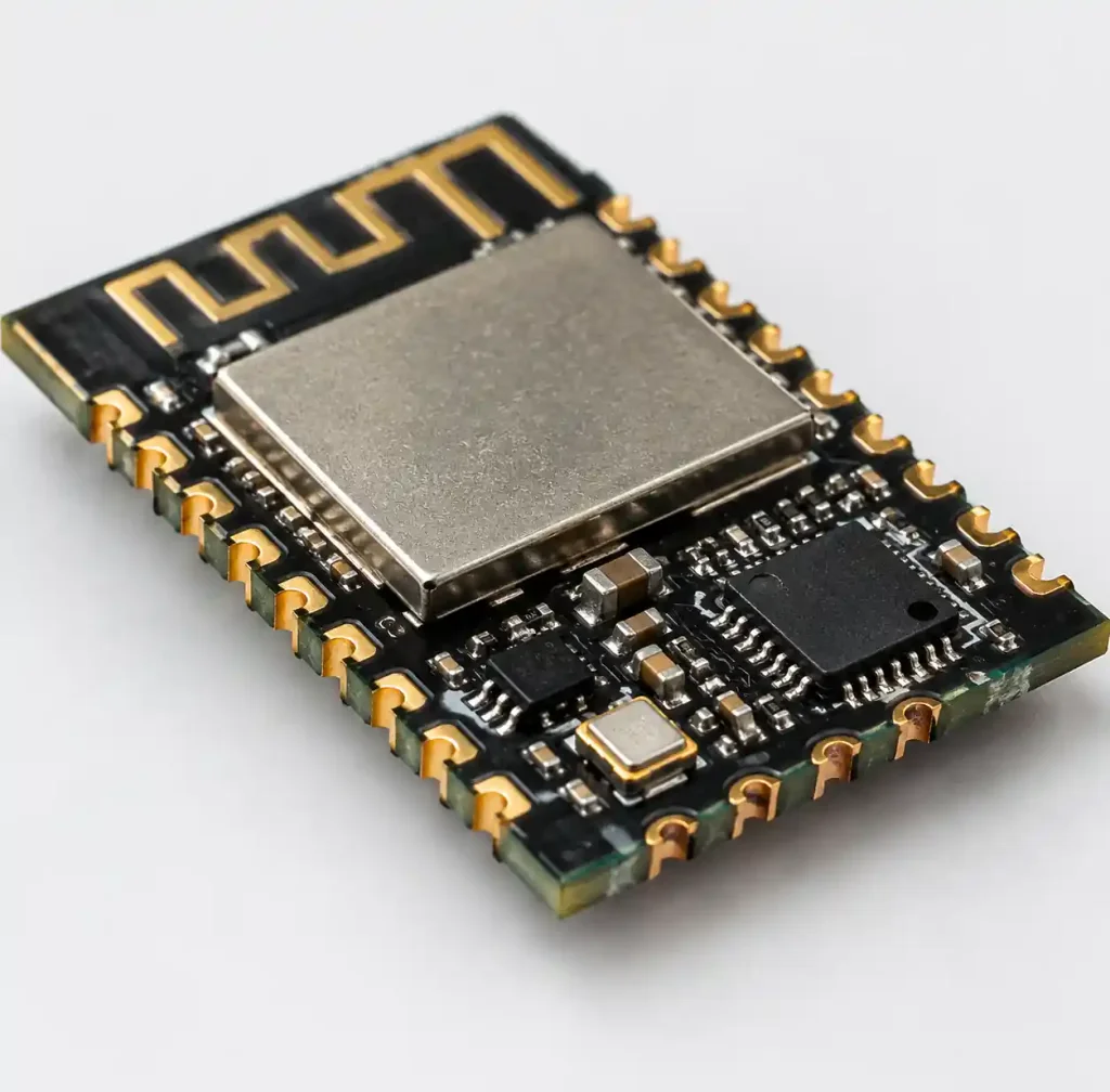
What Are Castellated Holes?
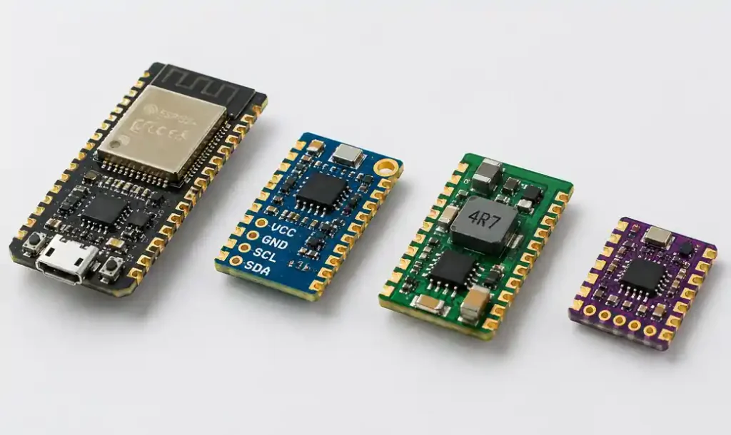
Castellated holes are plated half-holes located along the edge of a PCB, creating semi-circular copper-plated notches that enable surface mount attachment to another board. The term “castellated” comes from their resemblance to castle battlements when viewed from the side.
Unlike standard through-holes that connect layers within a board, castellated holes serve as edge-mount connection points. The manufacturing process drills complete plated through-holes, then routes the board outline through the hole centers, splitting each hole precisely in half. The exposed copper-plated barrel becomes the solderable connection surface.
You commonly find castellated holes on breakout boards, RF modules (ESP32, nRF52), USB-to-serial adapters, Bluetooth modules, and sensor breakout boards. They replace traditional connectors, reducing assembly height by 2-4mm and eliminating the 50-70¢ connector cost per unit.
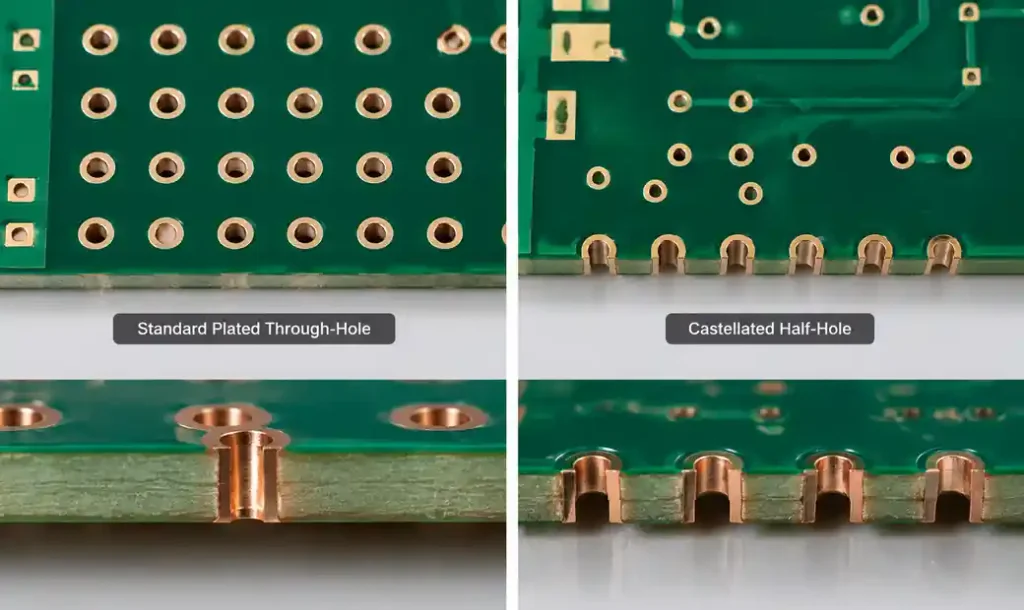
Castellated Holes vs Edge Plating
Both methods create edge connections, but differ in structure, cost, and reliability.
| Feature | Castellated Holes | Edge Plating |
|---|---|---|
| Structure | Half-holes with plated barrels | Continuous plated edge |
| Solder joint strength | Excellent (3-5× higher) | Good |
| Assembly difficulty | Moderate | Easy |
| Cost per board | $15-30 premium | $8-15 premium |
| Pitch capability | 0.8mm minimum | 0.5mm achievable |
| Visual inspection | Easy | Difficult |
| Rework capability | Excellent | Poor |
Castellated holes provide stronger mechanical bonds because solder forms a fillet around the semi-circular profile, creating interlocking geometry. Edge plating relies on flat surface wetting, offering 60% lower pull strength per IPC-7093 testing.
For high-reliability applications including automotive and medical devices, specify castellated holes. Edge plating works for low-stress consumer products where cost dominates.
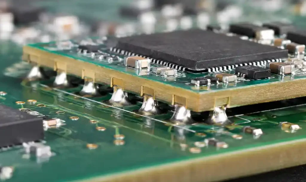
Design Rules for Castellated Holes
Hole Diameter and Spacing
Finished castellated hole diameter: 0.8-1.2mm for reliable plating. Smaller diameters (0.6mm) risk incomplete copper deposition in the barrel. Larger holes (1.5mm+) waste board space and weaken edge structure.
Minimum spacing between castellations: 2.54mm (0.1″) provides sufficient edge strength while allowing standard 0.1″ header compatibility. For 2.0mm pitch designs, increase board thickness to 1.2mm minimum or add edge support rails during routing.
Hole-to-edge distance: 1.0-1.5mm from hole center to board edge after routing. This leaves 0.25-0.55mm material remaining on each side of the hole, preventing edge delamination while ensuring clean half-hole geometry.
Pad Design and Annular Ring
Pad diameter for castellated holes: finished hole diameter + 0.4-0.6mm. For a 1.0mm hole, specify 1.5mm pad. This provides 0.25mm annular ring after routing—sufficient for reliable plating connection.
Use NSMD (Non-Solder Mask Defined) pads with soldermask opening 0.15mm larger than copper pad. For 1.5mm copper pad, specify 1.65mm mask opening. This exposes adequate copper for visual inspection while protecting inner traces.
Extend pads 1.5-2.0mm inboard from castellated edge to provide secure attachment for the mating board’s solder fillet. Surface tension draws solder across this pad extension, creating a robust T-joint configuration.
Plating Thickness Requirements
Copper plating thickness in castellated holes must meet IPC-6012 Class 2 minimum: 20μm (0.8 mil) average, 18μm minimum at any point. Class 3 applications require 25μm average for enhanced reliability under thermal cycling.
Standard PCB processes deposit 18-25μm plating. For castellated holes, verify with manufacturer that edge routing doesn’t expose areas below minimum thickness. Some shops apply secondary plating after routing to ensure full coverage.
Insufficient plating causes solder joint cracking after 200-500 thermal cycles (-40°C to +85°C per JESD22-A104). ESP32 modules with 15μm edge plating showed 18% failure rate versus 2% with proper 25μm plating in automotive qualification testing.
Manufacturing Process and Tolerances
The castellated hole fabrication sequence determines final quality and affects manufacturability.
Process steps: (1) Drill complete through-holes at specified locations, (2) Clean and desmear to prepare barrel for plating, (3) Electroless copper deposition followed by electroplating to achieve 18-25μm thickness, (4) Apply outer layer copper, pattern, and soldermask, (5) Route board outline through hole centers using precision CNC with ±0.1mm tolerance, (6) Final inspection for plating integrity and geometry.
Critical control point: routing depth and centering accuracy. The router bit must pass exactly through hole center, splitting it 50-50. Off-center routing by 0.15mm leaves 70% hole on one side and 30% on the other, creating uneven solder joints and potential shorts to adjacent pads.
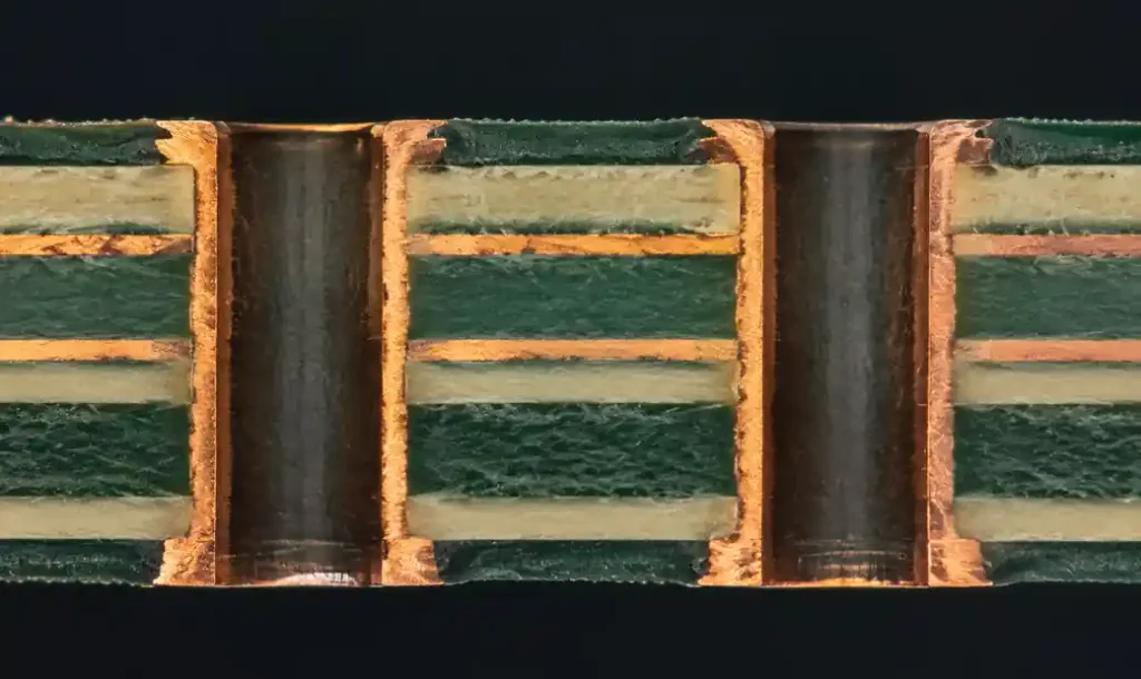
Manufacturing Tolerances
Board outline tolerance to drilled holes: ±0.1mm for castellated edges versus ±0.2mm for standard boards. Tighter control prevents asymmetric half-holes that cause assembly defects.
Castellated hole diameter tolerance: ±0.075mm (±3 mil) maintains consistent pad-to-hole geometry. Diameter variation above ±0.1mm disrupts annular ring calculations, risking insufficient copper connection.
Edge plating uniformity: maximum 20% thickness variation around castellated barrel per IPC-6012. Thin spots create weak points where thermal stress concentrates, initiating cracks that propagate under vibration.
Assembly Considerations
Solder Paste and Stencil Design
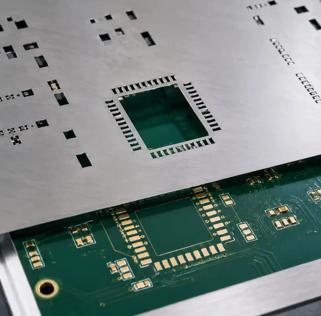
Castellated modules require modified stencil design compared to standard SMT. Aperture width: 90-100% of exposed pad width to deposit adequate paste volume. Length: extend apertures 1.2-1.5mm onto the parent board pad to ensure paste coverage across the joint interface.
Use Type 4 solder paste (25-45μm particle size) for 2.54mm pitch castellations. Finer pitches (2.0mm) require Type 5 paste (15-25μm particles). Solder paste volume must fill the castellated notch and create 0.3-0.5mm fillet height on the parent board pad.
Stencil thickness: 0.12-0.15mm (5-6 mil) provides optimal paste deposit for reliable joint formation. Thinner stencils (0.10mm) risk insufficient paste, while thicker (0.18mm) causes paste slump and bridging between adjacent castellations at 2.0mm pitch.
Reflow Profile and Thermal Management
Peak temperature: 245-255°C for SAC305 lead-free solder (Sn96.5Ag3.0Cu0.5). Time above liquidus (217°C): 60-90 seconds ensures complete wetting of castellated copper without overheating adjacent components on the module.
Preheat rate: 1-3°C/second to 150-180°C soak temperature prevents thermal shock that could crack ceramic components on modules. Soak duration 60-120 seconds allows flux activation and uniform heating across board mass differential.
Cooling rate: 2-4°C/second from peak to solidus prevents grain structure coarsening. Faster cooling (6-8°C/second) increases brittleness, raising crack risk under vibration per IPC-7095 reliability testing.
Common Assembly Defects
Insufficient solder at castellated joints: caused by inadequate paste deposit (volume 15-25% low) or poor wetting due to oxidation. Solution: increase aperture size by 10%, verify copper surface within 48 hours of routing, or specify ENIG surface finish for extended shelf life.
Solder bridging between castellations: occurs when paste volume exceeds 130% of calculated requirement or when pitch drops below 2.0mm with standard Type 4 paste. Solution: reduce aperture by 10%, switch to Type 5 paste for ≤2.0mm pitch, apply conformal soldermask.
Module tilting or tombstoning: results from uneven heating, asymmetric pad design, or off-center routing creating unequal solder joint areas. Solution: balance thermal mass around module, ensure ±0.1mm routing accuracy, verify pad symmetry in design.
Cracked plating at castellated edge: develops during thermal cycling when copper thickness falls below 18μm or board thickness exceeds 2.0mm without edge support. Solution: specify 25μm plating minimum, limit board thickness to 1.6mm for castellated edges, add internal copper ribs near edge for mechanical support.
Design Guidelines for Different Applications
WiFi/BLE modules (ESP32, nRF52): Use 2.54mm pitch castellations with 1.0mm diameter holes. These modules experience minimal mechanical stress but require solid RF grounding. Extend castellated ground pads 3-4mm inboard and connect to parent board ground plane through multiple thermal vias for RF shielding effectiveness.
Power modules (buck converters, LDOs): Specify 2.0mm pitch with 1.2mm diameter holes to handle 2-5A current per pad. Use 2oz copper weight minimum on module and parent board. Multiple parallel castellations distribute current, reducing resistive heating—four 1.2mm castellations in parallel handle 12-15A with ≤30mV drop at 80°C ambient temperature.
Sensor breakout boards (IMU, pressure, temperature): Design 2.54mm pitch for breadboard compatibility. Apply conformal coating after assembly to protect exposed castellated joints from moisture and contamination. Critical for outdoor installations where humidity cycling causes corrosion at solder-copper interface.
USB modules and signal converters: Use 2.0mm pitch to accommodate USB differential pairs and maintain compact form factor. Route USB data lines through inner castellations with adjacent ground castellations for controlled 90Ω differential impedance. Verify impedance with TDR testing on assembled modules.
Cost Analysis
Castellated hole pricing adds $15-30 per panel depending on hole count and board thickness. A 100×100mm panel with 24 castellations costs $18-25 premium over standard routing. Volume pricing reduces premium to $8-12 per panel at 500+ units.
Lead time impact: add 2-3 days to standard PCB fabrication for routing setup and inspection. Quick turn services typically extend from 3-day to 5-7 day delivery when castellations are specified.
Assembly cost reduction: eliminating connectors saves $0.50-0.70 per unit in component cost plus $0.15-0.25 in placement and soldering time. At 1000 units, total savings reach $650-950, easily offsetting the castellated hole fabrication premium.
Rework advantage: castellated modules can be removed and replaced using hot air rework stations without special tooling. Connector-based modules require desoldering all pins simultaneously, often damaging parent board pads. Rework yield for castellated assemblies: 92-96% versus 75-82% for fine-pitch connectors.
FAQ
What is the minimum pitch for castellated holes?
2.0mm pitch represents the practical minimum for reliable production with standard manufacturing equipment. Some manufacturers achieve 1.5mm pitch using precision routing and tighter tolerances, but cost increases 40-60% and yield drops 8-12%. For ultra-compact designs requiring <1.5mm pitch, consider HDI microvias with buried connections instead of edge castellations.
Can castellated holes be used on boards thicker than 1.6mm?
Yes, but mechanical reliability decreases. Testing shows boards ≥2.0mm thickness experience 25-35% higher stress concentration at castellated edges during thermal cycling. Limit thickness to 1.6mm for standard castellations. For 2.0-2.4mm boards, add 0.8-1.0mm wide edge support rails that remain attached until after parent board assembly, then break away along scored tabs.
How do I specify castellated holes in PCB CAD software?
Place standard plated through-holes at the desired locations, then draw the board outline to intersect each hole center. In fabrication notes, specify “castellated holes per IPC-2221” and call out required copper plating thickness (20μm minimum, 25μm preferred). Include a detail view showing hole-to-edge dimension and pad geometry. Verify with manufacturer that their routing tolerance (±0.1mm typical) meets design requirements.
What surface finish works best for castellated holes?
ENIG (Electroless Nickel Immersion Gold) provides best shelf life and solderability for castellated edges—up to 12 months versus 3-6 months for HASL. The flat ENIG surface enables accurate solder paste printing on mating board pads. OSP (Organic Solderability Preservative) costs less but oxidizes within 6-8 weeks, requiring assembly shortly after module fabrication. Avoid HASL on castellated boards—uneven coating thickness (10-40μm variation) creates assembly difficulties.
Do castellated holes require special inspection?
Yes. Visual inspection verifies plating continuity and checks for routing accuracy. Use 10-20× magnification to examine copper barrel for thin spots, cracks, or delamination from substrate. Measure hole diameter with pin gauges (±0.075mm tolerance) and verify centering (half-hole should split 50-50, ±0.1mm). For Class 3 applications, perform cross-sectional microsection analysis on first article to verify 20-25μm plating thickness through entire castellated profile.
Can you add components near castellated edges?
Maintain 2.5mm minimum clearance from component body to board edge for routing tool clearance and to prevent component damage. Smaller components (0402, 0603) can be placed 1.5mm from edge if oriented parallel to edge direction. Never place tall components (electrolytic capacitors, connectors) within 5mm of castellated edge—these create shadowing during reflow that causes uneven heating and solder joint defects.
Conclusion
Castellated holes provide reliable, cost-effective board-to-board connections when designed with proper hole diameter (0.8-1.2mm), spacing (2.0-2.54mm pitch), and plating thickness (20-25μm). The manufacturing process requires precision routing through plated hole centers with ±0.1mm tolerance to ensure symmetrical half-holes and reliable solder joints. While castellations add $15-30 fabrication cost per panel, they eliminate $0.65-0.95 in connector costs per unit and enable 2-4mm height reduction in compact module designs. For production volumes above 500 units, total cost savings reach $500-800 while improving assembly yield and rework capability compared to fine-pitch connector alternatives.
At Andwin Circuits, we manufacture castellated PCBs with precision CNC routing, 25μm edge plating, and ±0.1mm tolerance control. Our IPC-6012 Class 2/3 certified facility produces WiFi modules, sensor boards, and power regulators with verified castellated hole quality for volumes from prototypes to 10,000+ units. Contact us for castellated PCB manufacturing and turnkey assembly services.