
Carbon Ink PCB: Conductive Ink Applications and Limitations
Carbon ink accounts for less than 5% of conductive materials used in PCB manufacturing, yet it solves specific design challenges that copper cannot address cost-effectively. Applications like membrane switches, edge connectors, and EMI shielding leverage carbon ink’s unique properties—oxidation resistance, wear tolerance, and lower processing temperatures—accepting trade-offs in conductivity for these functional benefits.
If you want to determine when carbon ink makes technical and economic sense for your PCB design, you must understand its electrical properties, printing processes, adhesion requirements, and design limitations compared to traditional copper traces. This guide explains carbon ink applications, conductivity data, manufacturing considerations, and hybrid design strategies based on current industry practices.
What Is Carbon Ink PCB?
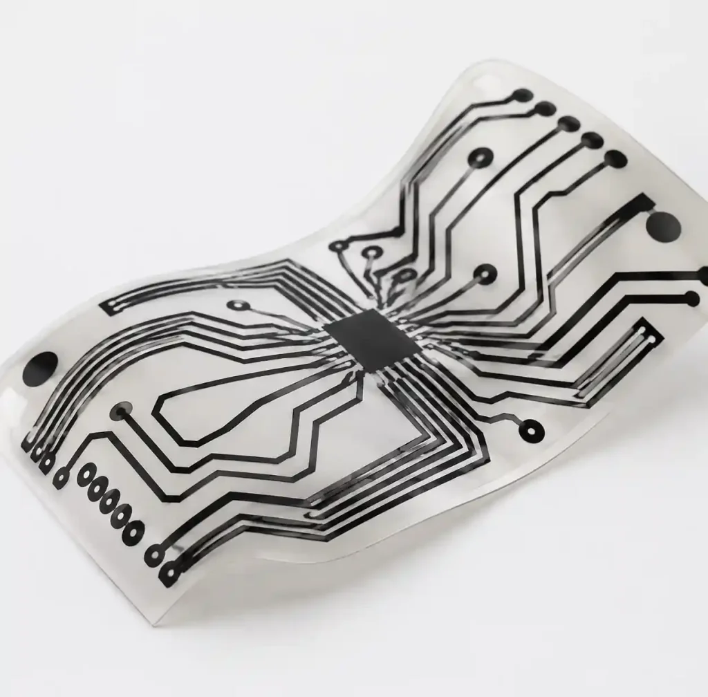
Carbon ink PCB refers to circuit boards where conductive carbon-based ink replaces or supplements copper in specific locations. The ink contains carbon particles (graphite, carbon black, or carbon nanotubes) suspended in a polymer binder, creating a printable conductive material that cures at 120-150°C. Unlike copper etching or plating, carbon ink is screen-printed or inkjet-printed directly onto substrates, forming functional conductive elements.
These PCBs serve applications where copper’s high conductivity is unnecessary or problematic. Carbon ink provides 10-100 ohms per square sheet resistance compared to copper’s 0.0005 ohms per square—sufficient for switches, resistive elements, and protective coatings but inadequate for power distribution or high-speed signals. You should specify carbon ink for low-current applications requiring wear resistance, cost reduction, or design flexibility that outweighs conductivity requirements.
Carbon Ink Applications in PCB Design
Membrane Switches and Tactile Interfaces
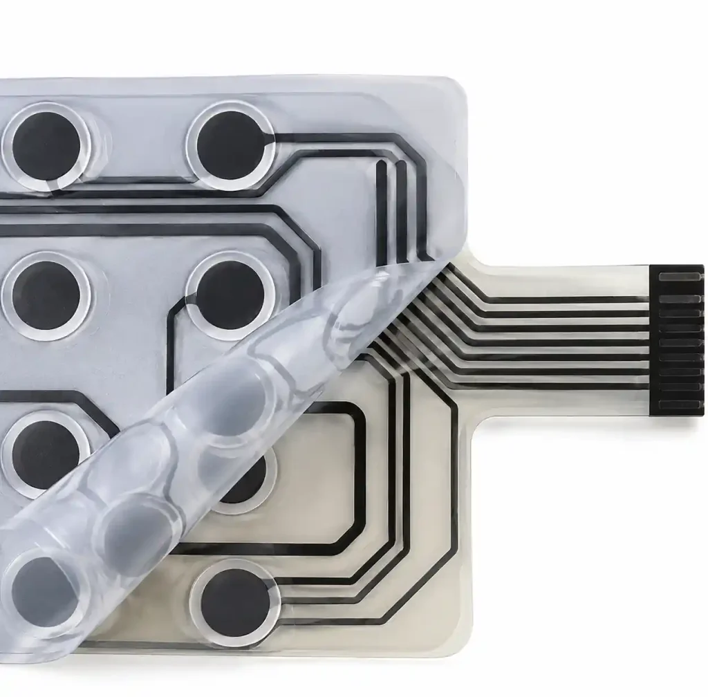
Carbon ink forms conductive traces in membrane switches for appliances, medical devices, and industrial controls. Sheet resistance of 20-50 Ω/sq provides adequate conductivity for low-current applications (<100mA) while delivering durability exceeding 1 million actuations. The flexible substrate deflects when pressed, connecting the carbon trace to the circuit below. This eliminates mechanical switches, reducing assembly costs by 30-40% and improving reliability to IP65 ratings.
Edge Connectors and Gold Finger Protection
Carbon ink protects copper edge fingers from oxidation and wear. A thin carbon layer (15-25 micrometers) over ENIG-finished connectors maintains contact resistance below 10 milliohms for 500+ mating cycles—costing 60-70% less than hard gold plating. The carbon acts as a sacrificial wear layer, protecting the underlying finish. Specify carbon ink edge protection for applications with 50-500 insertion cycles where hard gold is cost-prohibitive.
EMI Shielding and Resistive Heating
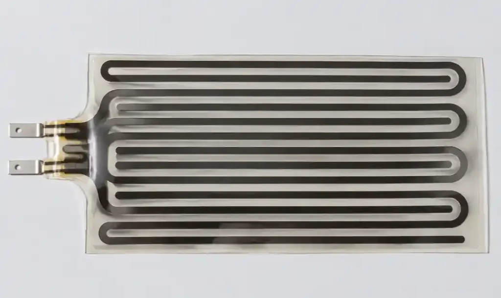
Carbon ink provides EMI shielding on flexible substrates with 20-40 dB attenuation from 100 MHz to 1 GHz. High-carbon formulations (>25% loading) with 50-100 micrometer thickness achieve 30-35 dB at 1 GHz—sufficient for consumer electronics while avoiding complex vacuum-deposited coatings. Carbon ink also enables printed resistive heaters with power densities of 0.1-0.5 W/cm². Automotive defoggers and medical warmers use carbon traces that withstand -40°C to +85°C, costing 40-50% less than wire-wound alternatives.
Carbon Ink vs Copper Conductivity Comparison
| Parameter | Carbon Ink | Copper (1oz) | Notes |
|---|---|---|---|
| Sheet Resistance | 10-100 Ω/sq | 0.0005 Ω/sq | Carbon 20,000-200,000× higher |
| Volume Resistivity | 0.001-0.01 Ω·cm | 1.68×10⁻⁶ Ω·cm | Application dependent |
| Current Capacity | <100 mA | 1-3 A per mm width | Carbon for low-current only |
| Oxidation Resistance | Excellent | Poor (requires finish) | Carbon inherently stable |
| Wear Cycles | >1M actuations | Degrades without protection | Carbon self-lubricating |
| Processing Temp | 120-150°C | 180-260°C (assembly) | Carbon suits thermoplastics |
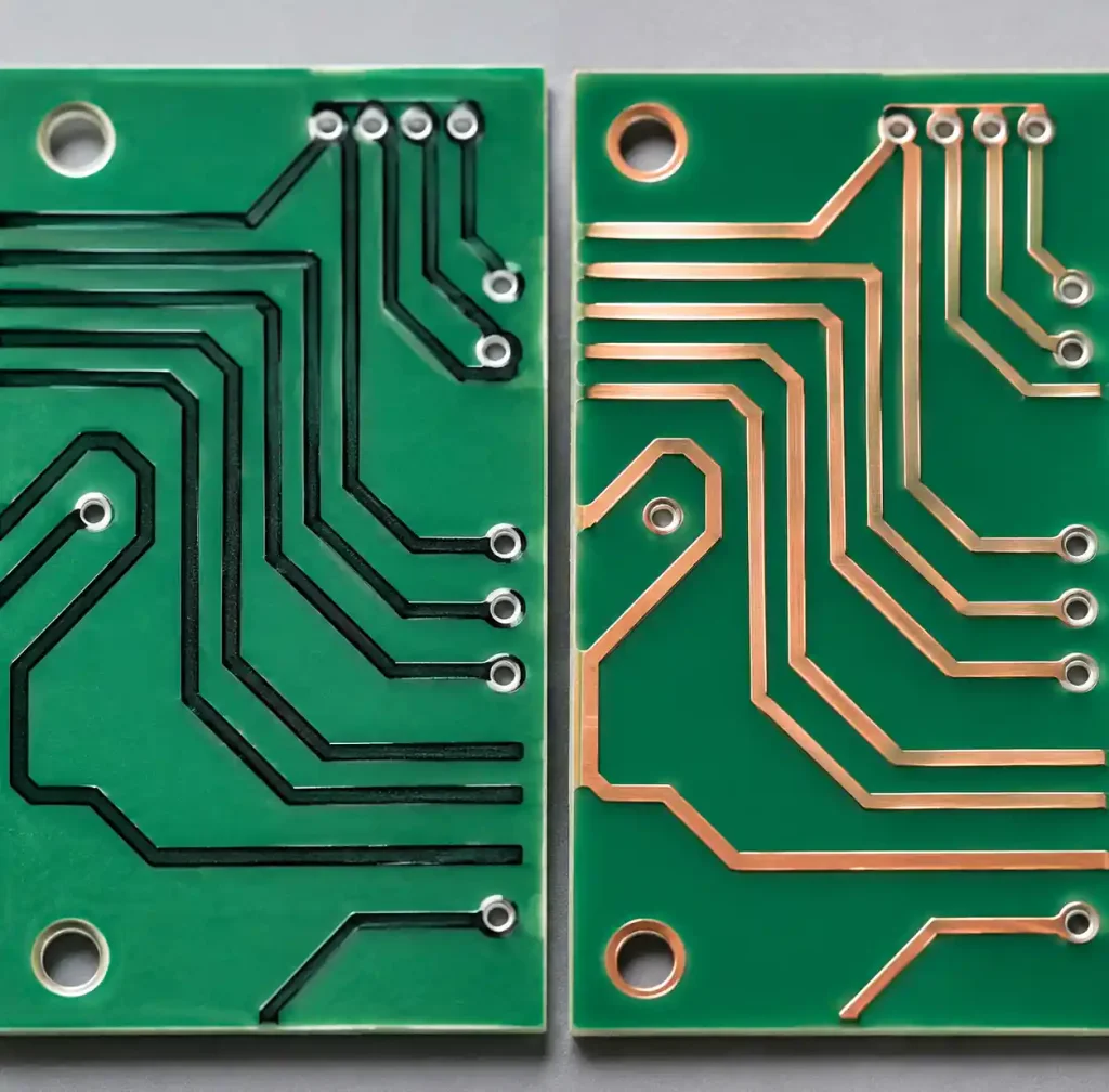
This comparison demonstrates carbon ink’s role as a specialty material, not a copper replacement. Conductivity limits carbon ink to applications where resistance values of 10-1000 ohms are acceptable or even desirable. Membrane switches operate at microamp to milliamp levels where voltage drops across carbon traces remain below 0.5V. Power distribution, high-speed signaling, and RF circuits require copper’s superior conductivity.
Carbon Ink Printing Processes
Screen Printing for Volume Production
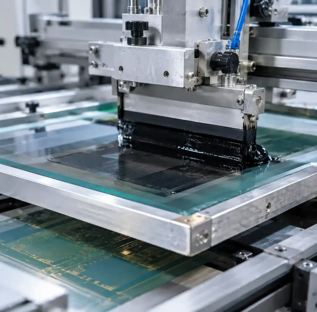
Screen printing deposits 15-50 micrometer carbon ink layers through patterned mesh, achieving 100-150 micrometer (4-6 mil) resolution with 200-325 mesh screens. Production rates reach 500-1000 prints per hour with automated equipment, making it cost-effective for volumes above 5,000 units. Inks require 5,000-15,000 cP viscosity with thixotropic additives. Curing occurs at 120-150°C for 10-20 minutes, crosslinking the binder while maintaining substrate integrity.
Inkjet Printing for Prototypes
Inkjet delivers maskless deposition with 50-100 micrometer resolution, eliminating screen fabrication for rapid prototyping below 500 units. Piezoelectric printheads dispense low-viscosity inks (5-20 cP) with <200nm particle sizes. Layer thickness builds through multiple passes, reaching 5-15 micrometers after 3-5 passes. Production speeds lag screen printing (100-200 units per hour), but zero setup costs justify inkjet for prototypes. Material costs run 2-3× higher than screen inks due to stringent particle control.
Design Limitations and Considerations
Adhesion and Substrate Compatibility
Carbon ink adhesion depends on substrate surface energy. Polyester (PET) and polyimide (PI) require corona or plasma treatment achieving >38 dynes/cm for reliable wetting. Adhesion testing per ASTM D3359 should demonstrate 5B rating (no peeling) after crosshatch tape testing. FR-4 and rigid substrates require surface roughening or adhesion promoters due to poor bonding with glossy soldermask. When printing over copper pads, specify an intermediate dielectric layer to prevent carbon-copper interaction degrading contact resistance.
Conductivity Stability and Current Limitations
Carbon ink resistance increases 0.05-0.2% per °C with 5-10% variation from -40°C to +85°C. Humidity exposure (85°C/85% RH for 1000 hours) increases resistance 10-15% without protective overcoats. Specify acrylic or urethane overcoats maintaining resistance within ±5% per IEC 60068-2-78. Current capacity is fundamentally limited—a 1mm wide, 25-micrometer thick trace with 50 Ω/sq carries only 10-20 mA continuous before excessive heating (>20°C rise) occurs. At 50 mA, a 500-ohm trace dissipates 1.25W, degrading the polymer binder. Never specify carbon ink for power distribution or high-current switching where copper is mandatory.
Hybrid Carbon-Copper PCB Design
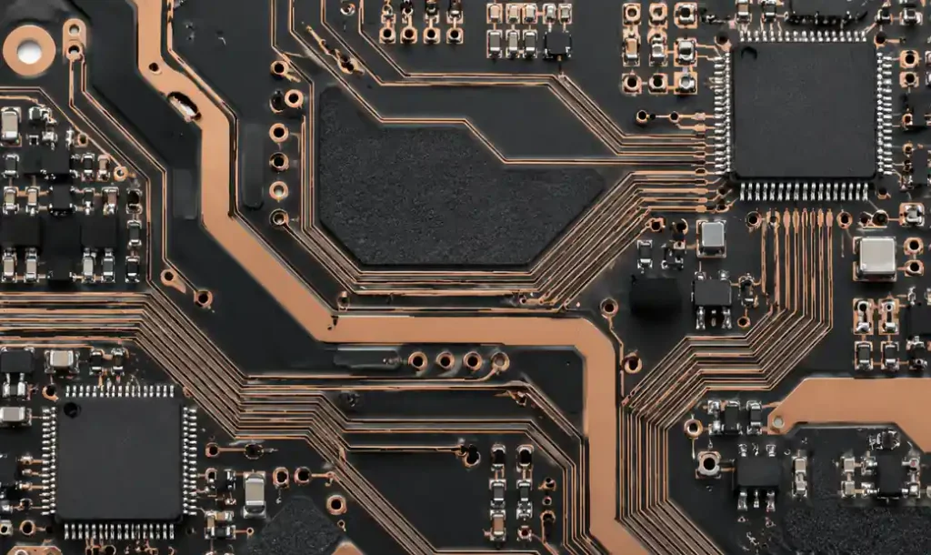
Hybrid designs integrate carbon ink and copper on the same PCB, leveraging each material’s strengths. Copper (0.5-1oz) handles power and signals while carbon ink provides switch contacts, edge protection, or resistive elements—reducing costs 20-30% compared to all-copper designs. Manufacturing adds a carbon printing step after soldermask application. Maintain 0.25-0.5mm clearance between carbon and copper features unless intentional contact is required. These guidelines ensure manufactururable designs with predictable performance. Provide carbon ink artwork on separate Gerber layers with clear documentation on formulation and curing requirements.
| Design Parameter | Minimum Value | Preferred Value | Notes |
|---|---|---|---|
| Trace Width | 0.2mm (8 mils) | 0.3-0.5mm | Narrower traces increase resistance |
| Trace Spacing | 0.2mm (8 mils) | 0.3mm+ | Prevents bridging during printing |
| Carbon-Copper Clearance | 0.25mm | 0.5mm | Avoid contamination |
| Layer Thickness | 15 μm | 25-35 μm | Multiple passes for thickness |
| Curing Temperature | 120°C min | 140-150°C | Substrate dependent |
When to Choose Carbon Ink PCB
Select carbon ink for low-current operation (<100mA), oxidation/wear resistance requirements, flexible substrates incompatible with copper plating, or cost sensitivity where simplified processing saves 30-50%. Proven applications include membrane switches, edge connectors, and EMI shielding. Avoid carbon ink for power distribution, high-speed signals, RF circuits above 1 GHz, or applications requiring <1 ohm contact resistance—copper delivers superior performance in these scenarios.
Frequently Asked Questions
What is the typical sheet resistance of carbon ink for PCB?
Carbon ink ranges from 10-100 Ω/sq depending on carbon loading. High-conductivity inks (10-30 Ω/sq) use carbon nanotubes for switches and edge connectors. Standard formulations (30-100 Ω/sq) employ carbon black for general purposes. Sheet resistance is measured per ASTM D257.
Can carbon ink replace copper traces?
Carbon ink cannot replace copper for most traces due to 20,000-200,000× higher resistivity. Use it as a specialty material for switches, protective coatings, and resistive elements while copper handles power and signals.
How many insertion cycles can carbon ink edge connectors withstand?
Carbon ink edge connectors withstand 500-1,000 cycles before contact resistance exceeds 10 milliohms—suitable for consumer electronics. Hard gold survives 10,000+ cycles but costs 300-400% more.
What printing process is best for carbon ink PCB?
Screen printing suits volumes above 5,000 units with 15-50 micrometer thickness. Inkjet serves prototypes and <500 units with 50-100 micrometer resolution but higher material costs (2-3× ink premium).
Does carbon ink work on flexible substrates?
Carbon ink works excellently on PET, PI, and PC at 120-150°C processing temperatures—below substrate thermal limits (PET: 150°C, PI: 300°C). Surface treatment (corona/plasma) may be required for 5B adhesion per ASTM D3359.
What environmental conditions affect carbon ink?
Temperature and humidity affect resistance. Expect 5-10% variation from -40°C to +85°C. Humidity (85°C/85% RH) increases resistance 10-15% over 1000 hours without overcoats. Specify acrylic or urethane overcoats per IEC 60068-2-78.
Conclusion
Carbon ink serves PCB applications where oxidation resistance, wear tolerance, and low processing temperatures deliver benefits despite conductivity limitations. With 10-100 Ω/sq sheet resistance versus 0.0005 Ω/sq for copper, carbon ink suits low-current circuits where resistance values up to 1,000 ohms are acceptable. Screen printing for volume and inkjet for prototypes determine manufacturing feasibility, while hybrid designs optimize cost and performance. Membrane switches, edge connector protection, EMI shielding, and resistive heaters represent proven applications with reliable data. You can specify carbon ink PCBs when electrical requirements align with material capabilities, accepting conductivity limitations for functional advantages copper cannot provide cost-effectively.
If you need PCB manufacturing with carbon ink capability for membrane switches or specialty applications, Andwin Circuits offers advanced hybrid PCB fabrication up to 50 layers with fast delivery in 7 days. Our facility handles carbon ink screen printing, flexible substrate processing, and copper-carbon hybrid designs, certified to ISO 9001 and IPC standards for consistent quality.
Contact us today for custom carbon ink PCB solutions and competitive factory-direct pricing.