Electronics PCB Assembly Manufacturing Process | Andwin
Printed Circuit Board (PCB) assembly is a crucial step in the manufacturing process of electronic devices.
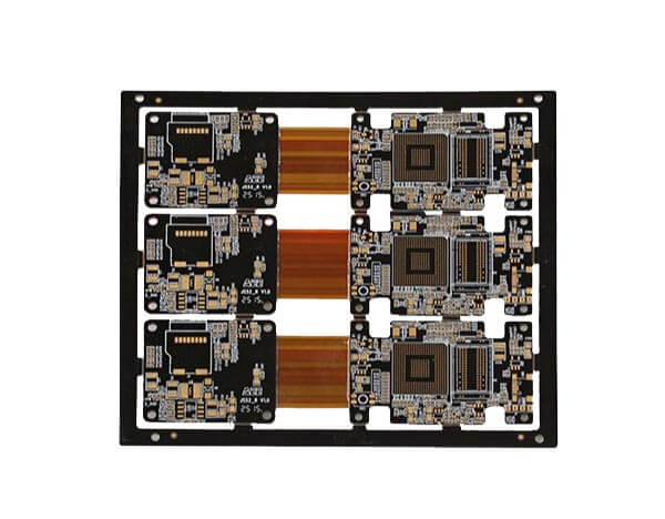
It involves the assembly of electronic components onto a PCB, which serves as the foundation for the device’s electrical system. The process of PCB assembly is a complex one, requiring precision and attention to detail.
The PCB assembly process can be broadly classified into two categories: Surface Mount Technology (SMT) and Through-Hole Technology (THT).
SMT is the most commonly used assembly method, and it involves the placement of surface-mount components onto the PCB. THT, on the other hand, involves the insertion of components through holes drilled into the PCB.
The PCB assembly process begins with the design of the PCB itself. The design is created using Computer-Aided Design (CAD) software, which allows the engineer to create a virtual representation of the PCB. Once the design is complete, it is sent to a PCB manufacturer, who produces the physical PCB.
The next step in the PCB assembly process is the application of solder paste to the PCB. Solder paste is a mixture of flux and solder particles that is applied to the pads on the PCB where the components will be placed. The solder paste is applied using a stencil, which ensures that the paste is applied only to the correct areas.
Once the solder paste has been applied, the components are placed onto the PCB. This is done using automated equipment, which picks up the components and places them onto the correct pads on the PCB. The components are held in place by the solder paste.
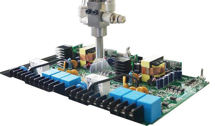
After the components have been placed, the PCB is heated in a reflow oven. The heat causes the solder paste to melt, forming a bond between the components and the PCB. This process is known as reflow soldering.
Once the PCB has been soldered, it is inspected to ensure that all of the components are correctly placed and soldered. This is done using automated inspection equipment, which checks for defects such as missing components or solder bridges.
After inspection, the PCB is tested to ensure that it functions correctly. This is done using automated testing equipment, which checks the electrical connections between the components on the PCB.

In conclusion, the PCB assembly process is a complex one that requires precision and attention to detail. It involves the design of the PCB, the application of solder paste, the placement of components, reflow soldering, inspection, and testing. The process is critical to the manufacturing of electronic devices, and any defects in the PCB assembly process can result in faulty devices. Therefore, it is essential to ensure that the PCB assembly process is carried out with the utmost care and attention to detail.