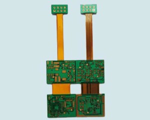
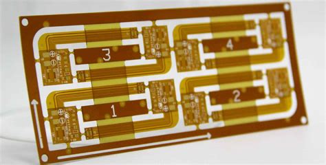
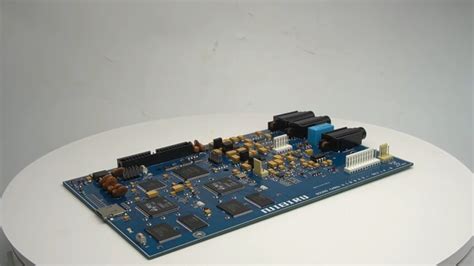
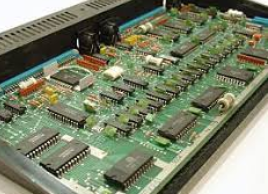
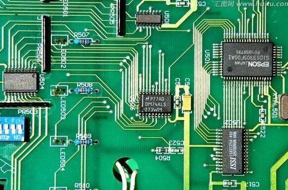
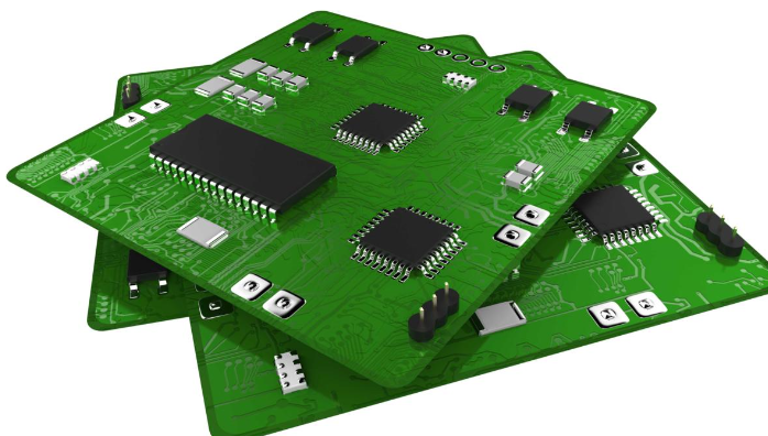
a printed circuit board
The difference between printed circuit boards and integrated circuit boards
Printed circuit boards are important electronic components, supporting electronic components and carriers for electrical connections of electronic components. Because they are made using electronic printing, they are called “printed” circuit boards.
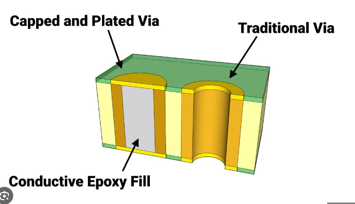
Current circuit boards are mainly composed of lines and patterns (Pattern), dielectric layers (Dielectric), holes (Through hole / via), solder resist ink (Solder resistant /Solder Mask), silk screen (Legend /Marking/Silk screen), surface treatment (Surface Finish), etc.
Advantages of PCB: high density, high reliability, designability, manufacturability, testability, assemblability, maintainability
What is an integrated circuit?
An integrated circuit (integrated circuit) is a microelectronic device or component. Using a certain process, the transistors, resistors, capacitors, inductors and other components and wiring required in a circuit are interconnected and made on a small piece or several small pieces of semiconductor wafers or dielectric substrates, and then packaged in a tube shell to become a microstructure with the required circuit function; all the components have formed a whole in structure, making electronic components a big step towards miniaturization, low power consumption, intelligence and high reliability. It is represented by the letter “IC” in the circuit.
Integrated circuits can be divided into three categories according to their functions and structures: analog integrated circuits, digital integrated circuits and digital/analog hybrid integrated circuits.
Integrated circuits have the advantages of small size, light weight, few lead wires and welding points, long life, high reliability, good performance, etc., and at the same time, low cost and easy mass production.
The relationship between PCB and integrated circuits
Integrated circuits generally refer to the integration of chips, such as the north bridge chip on the motherboard and the CPU inside, which are all called integrated circuits, and the original name is also called integrated circuits. PCB refers to the circuit board we usually see, and there are printed and soldered chips on the circuit board.
Understanding of the relationship between the two: Integrated circuits (ICs) are soldered on PCBs; PCBs are the carriers of integrated circuits (ICs).
Simply put, an integrated circuit is a general circuit integrated into a chip. It is a whole. Once it is damaged inside, the chip is also damaged. PCBs can solder components by themselves, and components can be replaced if they are damaged.
History of a printed circuit board
Before the advent of printed circuit boards, the interconnection between electronic components was based on direct wire connection to form a complete circuit.
Today, circuit breadboards only exist as effective experimental tools, while printed circuit boards have become an absolute dominant force in the electronics industry.
In the early 20th century, in order to simplify the production of electronic machines, reduce the wiring between electronic parts, and reduce production costs, people began to study the method of replacing wiring with printing.
Over the past thirty years, engineers have continuously proposed to use metal conductors on insulating substrates for wiring.
The most successful one was in 1925, when Charles Ducas of the United States printed a circuit pattern on an insulating substrate, and then printed a conductor circuit pattern on the insulating substrate by electroplating, which was called the additive method.
Until 1936, Austrian Paul Eisler published foil film technology in the UK. He used printed circuit boards in a radio device; in Japan, Yoshinosuke Miyamoto successfully applied for a patent for the spray wiring method.
Of the two, Charles Ducas and Miyamoto Kiyosuke only added the required wiring; Paul Eisler’s method is most similar to today’s printed circuit boards, which is to selectively apply a resist on an insulating substrate covered with metal foil and etch away unnecessary copper areas to prepare electronic circuits. This method is called the subtractive method.
However, because the electronic components at the time generated a lot of heat, the two substrates were difficult to use together, so they were not officially put into practical use. However, they also made printed circuit technology a step further.
In 1941, the United States painted copper paste on talc for wiring to make proximity fuses.
In 1943, Americans used this technology extensively in military radios.
In 1947, epoxy resin began to be used to manufacture substrates. At the same time, the National Bureau of Standards of the United States began to study the manufacturing technology of forming coils, capacitors, resistors, etc. using printed circuit technology.
In 1948, the United States officially recognized this invention for commercial use. Since the 1950s, transistors with lower heat generation have replaced vacuum tubes in large numbers, and printed circuit board technology has begun to be widely adopted. At that time, etching foil film technology was the mainstream
In 1950, Japan used silver paint on glass substrates for wiring; and copper foil on paper phenolic substrates (CCL) made of phenolic resin for wiring.
In 1951, the emergence of polyimide further improved the heat resistance of resins, and polyimide substrates were also manufactured.
In 1953, Motorola developed a double-sided board with electroplated through-holes. This method was also applied to later multi-layer circuit boards.
In the 1960s, 10 years after printed circuit boards were widely used, their technology became increasingly mature.
Since the advent of Motorola’s double-sided board, multi-layer printed circuit boards (MLB) began to appear, which further improved the ratio of wiring to substrate area.
In 1960, V. Dahlgreen used a metal foil film with printed circuits to stick to thermoplastic plastic to create a flexible printed circuit board.
In 1961, the Hazeltine Corporation in the United States made a multilayer board based on the electroplating through-hole method.
In 1967, the “Plated-up technology” was published as one of the build-up methods.
In 1969, FD-R used polyimide to manufacture flexible printed circuit boards.
In 1979, Pactel published the “Pactel method” as one of the build-up methods.
In 1984, NTT developed the “Copper Polyimide method” for thin-film circuits.
In 1988, Siemens developed a build-up printed circuit board with Microwiring Substrate.
In 1990, IBM developed a build-up printed circuit board with “Surface Laminar Circuit” (SLC).
In 1995, Panasonic developed a build-up printed circuit board with ALIVH.
In 1996, Toshiba developed B2it’s build-up printed circuit board.
At the end of the 1990s, when many build-up printed circuit board solutions were proposed, build-up printed circuit boards were officially put into practical use on a large scale.
Around the beginning of the 21st century, MLB and flexible printed circuit boards (FPC) developed rapidly, and the miniaturization of chip components and high-density installation methods increased the interconnection density of electronic products. In the 2020s, printed circuit boards continued to evolve towards high input/output (I/O) density, high precision (narrow line width/line spacing, Line/Space, L/S), and high integration, showing the characteristics of integrated integration and three-dimensional installation.