AC-DC controller PCB layout guide
In the application of 65W~150W output power range, CrM PFC+QR Flyback topology is a very commonly selected architecture. With the trend of miniaturized integrated circuits, QR combo control chips have emerged. In addition, for consumer electronic products, not only does energy efficiency need to meet regulatory requirements, but its standby loss is also a very important evaluation indicator.
The SO20 package not only integrates the functions of PFC and QR controllers, but also integrates high-voltage startup and X2 cap discharge mechanisms.
Of course, the IC must also consider the insulation and empty pin distance, so that some pins have complex functions, such as HV/X2, BO/X2, PCS/PZCD… Among them, PCS/PZCD is particularly sensitive to small signal detection, so as to avoid users from making inappropriate PCB layout designs when they should be careful but not pay attention, resulting in abnormal action protection triggering. The following will introduce the application experience and precautions related to NCP1937.
The NCP1937 integrates power factor correction (PFC) and quasi-resonant (QR) flyback controllers, designed for power adapters and high-efficiency, compact switching power supplies, such as PD fast charging, industrial communication power supplies, power tool fast charging, etc. This is an AC-DC device with a hybrid digital core architecture that provides higher energy efficiency, enhanced flexibility, and simplified system design applications. The PFC stage exhibits a power factor close to 1 when operating in critical conduction mode (CrM) with maximum frequency clamping. The circuit combines all the necessary functions required to build a rugged and compact PFC stage while minimizing the number of external components. The quasi-resonant current mode flyback stage has a proprietary valley lock circuit to ensure stable valley switching. The system operates to the fourth valley and switches to a frequency foldback mode with the minimum frequency clamped beyond the 4th order valley to eliminate audible noise. The skip cycle mode operation allows excellent efficiency under light load conditions with very low standby power consumption.
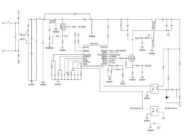
Figure 1 Application circuit of NCP1937 and the difference of various grounding points
1 Effect of current path and grounding point on noise
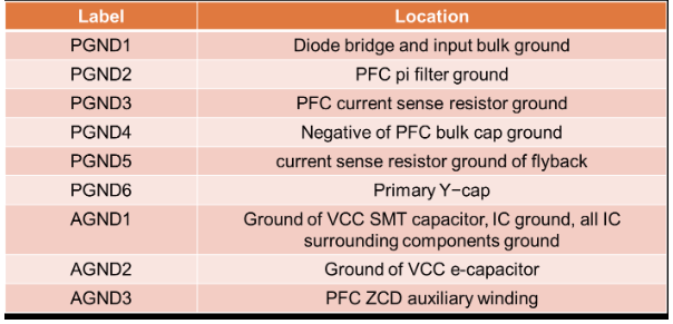
In any power converter, PCB layout and routing need to be considered to minimize noise generation and ensure stable operation. As a combo IC, NCP1937 controls two variable switching frequency converters and operates independently of each other. In fact, the gate driver of the PFC section and the gate driver of the QR section can be turned on and off at any point. Therefore, it is necessary to pay special attention to the current current path and grounding point to avoid noise interaction between the two converters. Before laying out the PCB for NCP1937, it is recommended to distinguish and annotate the various grounding points (as shown in Figure 1). Table 1 below illustrates the grounding points for different current paths and is denoted as PGNDx. At the same time, to distinguish the analog or signal grounding point, it is denoted as AGNDx. Star grounding is well known in the industry and is a good layout practice. Figure 2 is an example of the application circuit of NCP1937 with star grounding configuration on the primary side. The following is a description of the PCB layout and grounding points for the primary side current path:
1.1 Provide separate paths for the switching current of the PFC and flyback converters. As shown in Figure 1, the current path from PGND3 to PGND4 (PFC current path) and the current path from PGND4 to PGND5 (flyback converter current path) are completely separated and have their own current loops. This will avoid overlapping of the switching current and the gate drive current from the two converters.
Table 1 describes the various grounding points in Figure 1
1.2 The path between PGND6 and PGND4 can improve the surge tolerance. It is recommended to use a separate trace with sufficient line width to connect PGND6 back to PGND4.
1.3 It is recommended that the wiring between PGND4 and PGND5 be as short as possible.
1.4 PGND4 will be the star connection center point of the entire analog signal ground. The connection between PGND4 and AGND1 should be as short and as wide as possible.
1.5 PGND1, PGND2, and PGND3 can be continuous paths, that is, these paths do not need to be isolated.
PCB layout and grounding point description for primary side analog signals:
1) AGND1 is the star center point of the analog signal ground terminal. AGND2 and AGND3 should intersect at this point.
2) AGND3 comes from the auxiliary winding of the PFC choke and should be connected to AGND1 separately.
3) AGND2 should be connected to AGND1 separately.
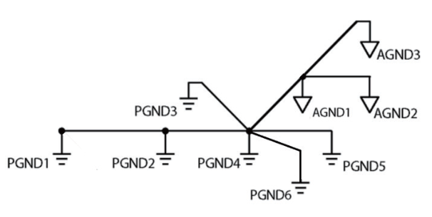
Figure 2 Example of using star grounding for NCP1937
2 Use case: PCB layout of 90W power adapter application circuit
Figure 3 is a demonstration board of the 90W power adapter of Onsemi. Next, the practical PCB layout method is further explained through the application circuit (Figure 4).
2.1 When placing NCP1937, the IC can be close to the PFC current sensing resistor.
2.2 The PFC current sensing resistor should be as close to the ground terminal of the bulk cap as possible.
2.3 It is recommended that the PCS/PZCD and QCS loops be routed first, and the path should be as short as possible. Any high-frequency drive signal and high dv/dt signal are prohibited from crossing or approaching the PCS/PZCD and QCS signal return path
2.4 PFC power current must return to Bulk cap GND alone. (Red power grounding)
2.5 Flyback power current must return to Bulk cap GND alone and cannot return to Bulk cap GND through the PFC power current path
2.6 The ground terminal of the auxiliary winding of the PFC choke must be directly connected to the ground terminal of the VCC SMT capacitor
2.7 VCC SMT capacitor and PCS/PZCD filter capacitor must be close to the IC GND
2.8 All small signal grounding must be connected to the VCCSMT capacitor first. That is, the ground end of the VCC SMT capacitor will be distributed in a star shape to all small signal groundings (blue grounding)
2.9 QR Aux winding GND must first be connected to the electrolytic capacitor of VCC, and then divided into two paths from the electrolytic capacitor to connect to the VCC SMT capacitor GND and Bulk cap GND (green grounding)
2.10 PCS/PZCD RC filter must be close to the IC pin (blue circle 1)
2.11 QCS RC filter must be close to the IC pin (blue circle 2)
2.12 QZCD high and low line compensation resistors are close to the IC pin
2.13 HV/X2 and HV/BO pins can reserve grounded high voltage filter capacitors (~ 470pF)
2.14 The primary and secondary Y caps should be connected to the Bulk cap GND and output cap GND in separate loops, and should not be connected to the power loop or small signal grounding loop first.
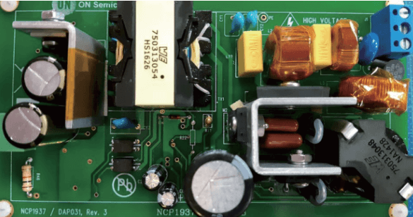
Figure 3 Display board of ON Semiconductor 90W power adapter
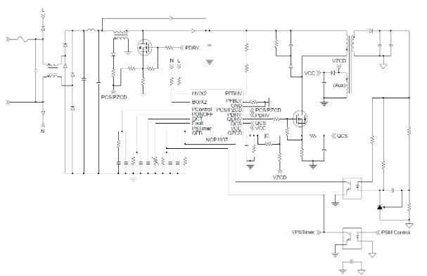
Figure 4 Application circuit and grounding layout
3 Optimize ESD through PCB layout to avoid false triggering of protection mechanism
On the other hand, in order to pass the ESD test, the path of ESD energy will be optimized through PCB layout to avoid false triggering of IC protection mechanism. Figure 5 is the grounding method before optimization. ESD energy will pass through the Y cap to the primary side and then return to the Bulk cap GND through an independent trace. However, when the other path is coupled to the primary side through the transformer winding, if the AUX winding grounding is first connected to the power trace of Current Sens, the CS signal will be distorted by the ESD injection energy, causing the OCP protection mechanism to be falsely triggered. However, the layout with better ESD performance, as shown in Figure 6, can be seen that not only will the Y cap go to the primary side through an independent trace back to the Bulk cap GND, but another path will be coupled to the primary side through the transformer winding. The AUX winding grounding will be connected to the Bulk cap GND first, which will prevent the CS signal from being distorted by the ESD injection energy and cause the OCP protection mechanism to be falsely triggered.
In short, for the Combo IC controller to operate two power converters, PCB layout is a key factor in the high efficiency and stable operation of the power converter. Following the above grounding recommendations will effectively reduce the noise coupling of one converter to the sensitive control signal of other converters.
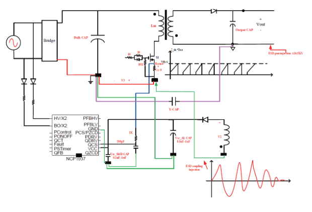
Figure 5 Before optimization, the GND of the auxiliary power winding is connected to the negative end of the PFC current sensing resistor
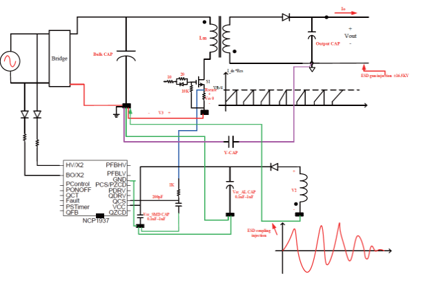
Figure 6 After optimization, the GND of the auxiliary power winding is connected to the negative end of the PFC bulk capacitor


