Additive Manufacturing Innovations in High-Density PCB Fabrication

Key Takeaways
When exploring PCB manufacturing advancements, you’ll find that additive manufacturing (AM) introduces transformative efficiencies. By enabling complex geometries and ultra-fine traces, AM empowers PCB manufacturing companies to achieve higher component density without compromising reliability. This approach reduces PCB manufacturing cost by minimizing material waste and accelerating prototyping—critical for staying competitive in the PCB manufacturing business.
You’ll notice that AM’s layer-by-layer fabrication supports multilayer architectures previously unattainable with traditional methods. While subtractive techniques remain vital for mass production, AM complements them by offering rapid iteration for high-density designs. For instance, integrating conductive inks or advanced polymers through AM allows precise control over dielectric properties, addressing challenges like signal loss in compact layouts.
Crucially, AM’s design flexibility lets you experiment with embedded components or non-planar structures, unlocking innovation cycles. However, balancing scalability and material performance remains a focus—ensuring AM’s role evolves from prototyping to mainstream PCB manufacturing. By strategically blending AM with conventional processes, you can optimize both speed and precision, positioning your operations at the forefront of next-gen electronics.

Enhancing PCB Density with AM
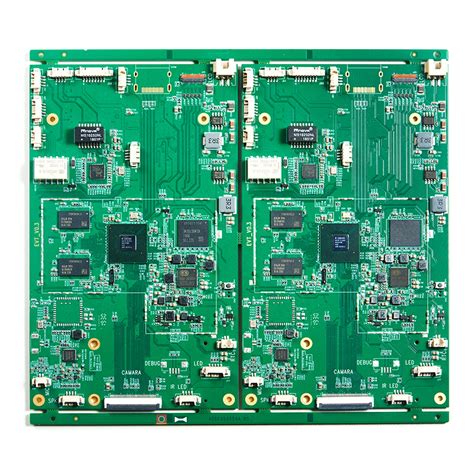
When exploring PCB manufacturing solutions, you’ll find additive manufacturing (AM) unlocks unprecedented opportunities to enhance circuit density. Unlike traditional subtractive methods, AM builds multilayer architectures layer by layer, enabling finer traces and tighter spacing. This precision allows PCB manufacturing companies to embed components vertically, reducing footprint while increasing functionality—a critical advantage for miniaturized devices.
By integrating AM, you can bypass many constraints of conventional processes, such as etching limitations or alignment errors. For instance, 3D-printed conductive inks and dielectric materials enable embedded passives and interconnects within stacked layers, optimizing space utilization. This approach not only improves performance but also lowers PCB manufacturing cost by minimizing material waste and reducing post-processing steps.
However, balancing speed and resolution remains a challenge. While AM accelerates prototyping cycles, achieving sub-50-micron features demands advanced printers and specialized materials. Still, hybrid workflows—combining AM with traditional lamination—are emerging as a cost-effective strategy. This synergy lets you prototype high-density designs rapidly before scaling with established methods, making AM a strategic asset for any PCB manufacturing business aiming to stay competitive.
For deeper insights into optimizing AM workflows, explore industry benchmarks. By focusing on material innovation and process refinement, you can overcome density barriers while maintaining compatibility with existing production ecosystems.
3D Printed Multilayer PCB Designs
When designing high-density PCBs, you’ll find that additive manufacturing (AM) opens doors to geometries previously unachievable with traditional methods. Unlike subtractive processes that etch away copper layers, 3D printed multilayer PCB designs build conductive and dielectric layers sequentially, enabling tighter interlayer spacing and embedded components. This approach reduces pcb manufacturing cost by minimizing material waste and eliminating the need for multiple lamination cycles.
For pcb manufacturing companies, AM offers a strategic advantage in prototyping complex architectures. For instance, you can integrate vertical interconnects or non-planar traces without relying on costly photolithography tools. A comparison of key parameters highlights these benefits:
| Parameter | AM-Based PCBs | Traditional PCBs |
|---|---|---|
| Minimum Layer Spacing | 10–20 µm | 50–100 µm |
| Material Utilization | 95–98% | 60–75% |
| Tooling Lead Time | 1–3 days | 2–4 weeks |
Tip: To maximize ROI in your pcb manufacturing business, combine AM for rapid iteration of high-complexity designs with traditional methods for large-scale production. This hybrid model balances speed and economies of scale.
The design flexibility of 3D printed multilayer PCBs also allows for functional integration, such as embedding antennas or sensors within the board itself. By adopting AM, you can address signal integrity challenges in high-frequency applications while reducing pcb manufacturing bottlenecks caused by multi-step processes. However, material selection remains critical—ensure dielectric pastes and conductive inks meet your thermal and electrical performance requirements.
Rapid Prototyping via AM Techniques
When developing high-density PCBs, PCB manufacturing timelines often clash with the need for iterative design validation. Additive manufacturing (AM) disrupts this cycle by enabling rapid prototyping—compressing weeks of traditional fabrication into days. By layering conductive and dielectric materials directly from digital designs, you bypass complex lithography or etching steps, accelerating functional testing of multilayer architectures. For PCB manufacturing companies, this means faster feedback loops, reducing time-to-market for advanced electronics.
The cost dynamics shift significantly, too. AM eliminates tooling expenses tied to conventional PCB manufacturing business models, making low-volume prototyping economically viable. You can test multiple design permutations without inflating PCB manufacturing cost, ensuring optimal signal integrity and thermal performance before scaling. Material efficiency further lowers waste, as AM deposits materials only where needed.
This agility is critical when addressing evolving industry standards. By integrating AM early, you gain flexibility to refine trace geometries, via placements, or substrate configurations—key advantages for overcoming density challenges in next-gen devices. The synergy between AM and traditional methods isn’t just additive; it’s transformative, reshaping how prototypes evolve into production-ready solutions.
AM-Traditional PCB Method Synergy
When integrating additive manufacturing (AM) into PCB manufacturing, you’re not replacing traditional methods but enhancing their capabilities. Traditional PCB manufacturing companies often rely on subtractive processes like etching, which excel at high-volume production but struggle with ultra-fine geometries. By contrast, AM enables rapid iteration of high-density PCB designs—think embedded vias or non-planar circuits—while slashing PCB manufacturing cost during prototyping. For instance, printing a multilayer test board in hours instead of weeks lets your team validate concepts before committing to costly tooling.
The real advantage lies in hybrid workflows. Use AM to create intricate interconnects or antenna arrays, then combine these with mass-produced substrates via traditional lamination. This approach reduces material waste and accelerates time-to-market for specialized applications like IoT sensors or aerospace systems. Even for established PCB manufacturing businesses, blending AM with conventional techniques unlocks scalable flexibility—low-volume, high-complexity orders can coexist with bulk production lines. The key is balancing precision and economics: AM handles the “impossible” geometries, while subtractive methods ensure cost efficiency at scale.
This strategic integration allows you to address evolving market demands without overhauling existing infrastructure. By leveraging both technologies, your operations gain operational agility, ensuring competitiveness as device miniaturization and functional integration redefine PCB manufacturing standards.
Material Advances in PCB Additives
Recent breakthroughs in additive materials are reshaping how PCB manufacturing companies approach high-density designs. Innovations like conductive nanoparticle inks and dielectric polymers enable precise deposition of circuitry layers, eliminating the need for subtractive etching. These materials not only support finer traces—down to 15 µm—but also improve thermal stability, critical for multilayer architectures.
You’ll find that photo-curable resins now allow rapid curing under UV light, slashing production time for prototypes. This directly impacts PCB manufacturing cost, as material waste drops by up to 70% compared to traditional methods. Specialty substrates, such as ceramic-filled composites, further enhance heat dissipation in compact designs—a game-changer for high-power applications.
However, integrating these materials into existing PCB manufacturing business workflows requires careful calibration. For example, hybrid approaches combine additive layers with conventional plating to balance performance and scalability. As material libraries expand, expect tighter alignment between additive capabilities and the evolving demands of PCB manufacturing, from IoT devices to aerospace systems.
Design Flexibility in AM PCBs
Additive manufacturing (AM) redefines design possibilities in PCB manufacturing by enabling geometries that traditional methods struggle to achieve. Unlike subtractive processes, which rely on etching pre-laminated boards, AM builds circuits layer by layer, allowing you to integrate complex 3D structures and non-planar layouts. This eliminates constraints like fixed layer counts or rigid material choices, empowering PCB manufacturing companies to create high-density interconnects with embedded components or curved substrates.
The freedom to iterate rapidly reduces PCB manufacturing cost during prototyping, as design tweaks require minimal tooling changes. For instance, you can test multiple iterations of a multilayer design in hours rather than weeks—a critical advantage for startups or businesses scaling their PCB manufacturing business. AM also supports hybrid approaches, where intricate AM-built sections are combined with conventional PCB layers, balancing performance and affordability.
By embracing AM’s design flexibility, engineers can optimize signal paths, reduce electromagnetic interference, and consolidate components in ways that push the limits of miniaturization. This adaptability not only accelerates innovation but also positions AM as a complementary tool in the broader electronics production ecosystem.
Overcoming PCB Density Challenges
As PCB manufacturing pushes toward higher component density, traditional subtractive methods face physical limits in etching ultra-fine traces and microvias. Additive manufacturing (AM) circumvents these barriers by precisely depositing conductive inks layer-by-layer, enabling intricate geometries that bypass alignment errors inherent in multilayer lamination. This approach reduces PCB manufacturing cost by minimizing material waste—critical for high-mix, low-volume production common in prototyping.
For PCB manufacturing companies, AM unlocks the ability to embed passive components directly within dielectric layers, freeing surface space for active devices. This vertical integration slashes footprint while boosting signal integrity—a game-changer for compact IoT or wearable designs. However, transitioning to AM requires recalibrating design workflows; you’ll need simulation tools to optimize thermal management in densely packed 3D architectures.
By blending AM with hybrid workflows, PCB manufacturing businesses can scale complex designs without sacrificing yield. For instance, AM-printed interconnects complement traditional FR-4 substrates, balancing performance and affordability. As material science advances, expect AM to redefine density benchmarks while maintaining compatibility with existing assembly ecosystems.
Future Trends in AM PCB Development
As additive manufacturing (AM) evolves, you’ll see PCB manufacturing shift toward AI-driven design tools that optimize multilayer architectures for signal integrity and thermal management. Leading PCB manufacturing companies are experimenting with hybrid systems, blending AM’s rapid iteration capabilities with traditional processes to reduce PCB manufacturing cost while scaling production. Innovations like nanoparticle conductive inks and dielectric polymers will enable finer trace resolutions, directly addressing density bottlenecks that challenge conventional methods.
For PCB manufacturing businesses, sustainability will become a key differentiator. AM’s material efficiency—using up to 40% less substrate in complex designs—aligns with circular economy goals, while in-situ quality monitoring minimizes waste during printing. Additionally, decentralized production models, powered by AM, could shorten supply chains, letting you prototype and produce high-density boards locally.
The integration of machine learning for predictive maintenance in AM systems will further streamline workflows, ensuring consistency across batches. As these trends converge, AM won’t replace traditional techniques but will instead complement them, offering a flexible toolkit for balancing speed, cost, and complexity in next-gen electronics.
Conclusion
As you evaluate the evolving landscape of PCB manufacturing, additive techniques are proving indispensable for balancing innovation with practicality. By integrating 3D-printed multilayer architectures, PCB manufacturing companies can now address high-density challenges that once bottlenecked traditional methods. This synergy reduces PCB manufacturing cost while accelerating prototyping—a critical advantage in competitive markets where time-to-market defines success.
The flexibility of additive processes allows you to experiment with novel materials and intricate geometries, empowering PCB manufacturing businesses to meet rising demands for miniaturization without compromising performance. Yet, these advancements don’t replace conventional workflows; instead, they augment them, creating hybrid systems that leverage the precision of subtractive methods with the agility of additive solutions.
Looking ahead, the fusion of these technologies will likely redefine industry benchmarks, enabling you to tackle complex designs with unprecedented efficiency. Whether optimizing PCB manufacturing for IoT devices or high-frequency applications, the strategic adoption of additive manufacturing ensures your workflows remain adaptable, scalable, and future-ready.
FAQs
How does additive manufacturing reduce pcb manufacturing cost compared to traditional methods?
By eliminating the need for multiple tooling steps and minimizing material waste, pcb manufacturing becomes more cost-effective for low-to-medium production runs. This is especially valuable for prototyping, where design iterations can be tested without expensive setup fees.
Can pcb manufacturing companies integrate additive processes with existing workflows?
Yes, many pcb manufacturing businesses now combine additive techniques like 3D printing with subtractive processes. This hybrid approach optimizes high-density interconnects while maintaining compatibility with conventional assembly lines, ensuring seamless scalability.
Is additive manufacturing suitable for high-volume pcb manufacturing?
While AM excels in rapid prototyping and complex geometries, traditional methods remain more efficient for mass production. However, advancements in multi-material printing and automation are narrowing this gap, offering future potential for high-volume pcb manufacturing.
What design freedoms does AM offer for high-density pcbs?
You can create embedded components, non-planar circuits, and ultra-fine traces that are challenging with etching. This flexibility allows pcb manufacturing companies to meet evolving demands for miniaturization and performance in aerospace or medical devices.
How do material choices impact pcb manufacturing cost in AM?
Specialized conductive inks and dielectric polymers may initially raise material costs, but they reduce post-processing expenses. Over time, as material availability grows, pcb manufacturing businesses expect these costs to stabilize competitively.
Explore Advanced PCB Manufacturing Solutions
For tailored additive manufacturing options that align with your project’s needs, please click here to connect with industry-leading experts.