Advanced Charger PCB Manufacturing for Reliable Power Solutions
Key Takeaways
When selecting PCB manufacturing partners for charger systems, you need to prioritize expertise in high-current applications and thermal management. Leading PCB manufacturing companies leverage automated optical inspection (AOI) and impedance control to ensure reliability in power-intensive environments like EV charging. Balancing PCB manufacturing cost with quality requires evaluating material choices—such as high-frequency substrates or thermal-resistant laminates—and scalable production processes.
Tip: Always prioritize design-for-manufacturing (DFM) principles during prototyping to minimize PCB manufacturing cost while maintaining performance standards.
For businesses entering the PCB manufacturing business, understanding compliance with UL certification and IPC-6012 standards is non-negotiable. Advanced firms integrate laser drilling and sequential lamination to achieve compact, multi-layer designs essential for modern charging systems. By partnering with specialists, you gain access to real-time testing protocols and supply chain optimization, which streamline timelines without compromising on durability. This strategic approach ensures your charger PCBs meet both technical demands and market expectations efficiently.
EV Charger PCB Manufacturing Essentials
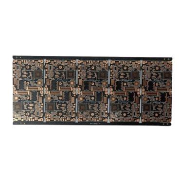
When designing PCB manufacturing processes for electric vehicle (EV) chargers, you need to prioritize durability, thermal management, and signal integrity. PCB manufacturing companies must balance pcb manufacturing cost with performance, especially when dealing with high-voltage applications. Key considerations include material selection (e.g., FR-4 or high-Tg substrates), copper thickness optimization, and adherence to IPC-6012 standards for reliability.
Here’s a breakdown of critical factors in EV charger PCB production:
| Factor | Impact |
|---|---|
| Layer Count | Determines power distribution complexity |
| Thermal Management | Prevents overheating in fast-charging systems |
| Material Quality | Ensures longevity under high-stress conditions |
To stay competitive in the pcb manufacturing business, manufacturers often leverage automated testing and advanced assembly techniques. For example, [automated optical inspection (https://www.andwinpcba.com) helps detect micro-defects early, reducing long-term failure risks. Additionally, integrating embedded components can minimize signal loss, which is crucial for maintaining efficiency in high-performance charging systems.
By collaborating with experienced PCB manufacturing companies, you gain access to tailored solutions that align with industry certifications like UL 62368-1. This ensures your EV charger PCBs meet both safety benchmarks and evolving market demands.
Precision Design for Reliable Charger PCBs
When developing charger systems, PCB manufacturing begins with optimizing circuit layouts to handle high currents and thermal stresses. Leading PCB manufacturing companies prioritize multi-layered designs with controlled impedance, ensuring stable power delivery across charging cycles. You’ll find that advanced techniques like thermal via arrays and copper balancing mitigate heat buildup, extending component lifespan while maintaining efficiency.
Balancing PCB manufacturing cost with performance requires meticulous material selection—high-Tg laminates and heavy copper substrates are common for durability. Automated optical inspection (AOI) and impedance testing further validate design accuracy, reducing failure risks in EV applications. For businesses scaling their PCB manufacturing business, investing in precision design tools and DFM (Design for Manufacturing) protocols ensures compatibility with automated assembly lines, streamlining production without compromising quality.
By collaborating with experienced partners, you gain access to signal integrity simulations and EMI shielding strategies that refine layouts for noise reduction. This approach not only aligns with industry standards but also future-proofs your charger systems against evolving power demands.
Competitive Charger PCB Assembly Pricing
When evaluating PCB manufacturing partners for charger assembly, understanding cost drivers is critical. Leading PCB manufacturing companies leverage economies of scale and advanced automation to optimize PCB manufacturing cost, ensuring affordability without compromising quality. By partnering with material suppliers and refining production workflows, these firms reduce overheads—savings they pass on to clients. For instance, high-volume orders for EV charger circuit boards often benefit from tiered pricing models, while design optimizations (like panelization) minimize material waste.
Cost-efficiency in PCB manufacturing business hinges on balancing precision and scalability. Advanced surface-mount technology (SMT) and rigorous testing protocols ensure reliability, even as prices remain competitive. You’ll find that reputable manufacturers offer transparent quotes, breaking down expenses for prototyping, component sourcing, and final assembly. This clarity helps you align budgets with performance requirements, whether you’re scaling production or refining prototypes.
Moreover, global supply chain partnerships enable access to premium materials at reduced rates, further lowering PCB manufacturing cost. By prioritizing value-driven solutions, top providers deliver durable, high-performance boards tailored to EV charging systems—proving that affordability and quality aren’t mutually exclusive in modern electronics manufacturing.
High-Performance EV Charging Systems Guide
When designing high-performance EV charging systems, understanding the role of PCB manufacturing becomes critical. These systems demand circuit boards capable of handling high voltages, rapid heat dissipation, and consistent power delivery. Leading PCB manufacturing companies leverage advanced materials like high-Tg laminates and copper-heavy substrates to ensure durability under extreme operational conditions.
Balancing PCB manufacturing cost with performance requirements is key—opting for multi-layered designs with precision-etched traces optimizes conductivity while minimizing energy loss. For businesses, partnering with a PCB manufacturing business that specializes in EV applications guarantees access to industry-specific testing protocols, such as thermal cycling and impedance control.
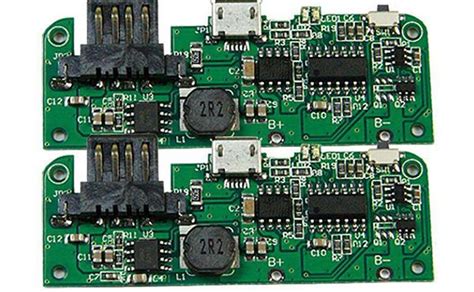
You’ll want boards that integrate smart charging features, like load balancing and fault detection, which rely on flawless signal integrity. Transitioning to automated assembly processes not only reduces human error but also scales production efficiently. By prioritizing collaboration with experienced manufacturers, you ensure your charging systems meet evolving industry standards while maintaining competitive pricing structures.
Expert Solutions for Charger Circuit Boards
When selecting PCB manufacturing companies for charger circuit boards, you need partners who understand the intricate balance between performance, durability, and PCB manufacturing cost. Leading providers combine precision engineering with advanced materials to optimize thermal management, current handling, and signal integrity—critical factors for high-power charging systems. For instance, in EV charger PCBs, multi-layer designs with copper-heavy substrates ensure efficient heat dissipation, while automated optical inspection (AOI) systems maintain consistency across large-scale production runs.
A well-structured PCB manufacturing business prioritizes design-for-manufacturability (DFM) principles to minimize errors and reduce turnaround times. By leveraging technologies like impedance-controlled routing and surface finishes such as ENIG (Electroless Nickel Immersion Gold), manufacturers enhance reliability in demanding environments. Cost optimization doesn’t mean compromising quality; instead, it involves strategic material selection and process automation to align with your project’s budget and scalability needs.
Whether you’re developing compact consumer chargers or industrial-grade EV charging systems, collaborating with experienced PCB manufacturing specialists ensures your designs meet regulatory standards and performance benchmarks. Their expertise in prototyping, testing, and volume production streamlines the journey from concept to market-ready solutions.
Advanced PCB Technology for Power Solutions
When selecting PCB manufacturing companies for power solutions like EV chargers, you need technology that balances precision and scalability. Modern PCB manufacturing leverages multi-layer designs with high-density interconnects (HDIs) to handle complex power distribution, ensuring minimal energy loss even under heavy loads. Advanced thermal management materials, such as metal-core substrates or ceramic-filled laminates, are critical for dissipating heat in high-current applications, directly impacting system longevity.
The PCB manufacturing cost often hinges on material selection and production techniques. While premium substrates like polyimide or FR-4HT may raise initial expenses, they reduce long-term failure risks—a vital consideration for mission-critical charging systems. Reputable PCB manufacturing business providers optimize costs through automated optical inspection (AOI) and design-for-manufacturability (DFM) checks, eliminating errors before mass production.
For EV charger applications, look for suppliers offering impedance-controlled routing and embedded component technology, which enhance signal integrity while shrinking board size. These innovations, paired with rigorous testing protocols, ensure your power solutions meet both performance benchmarks and industry certifications. By aligning with a PCB manufacturing partner skilled in these advanced methodologies, you secure boards that evolve alongside emerging energy demands.
Meeting Demands in EV Charger Manufacturing
As the adoption of electric vehicles accelerates, PCB manufacturing companies must address evolving technical and commercial challenges to deliver reliable charging solutions. Modern EV charger designs demand multilayered boards capable of handling high-voltage circuits, thermal management, and precise signal integrity. To stay competitive, manufacturers optimize PCB manufacturing cost without compromising quality—leveraging automated assembly lines and advanced materials like high-Tg laminates for durability.
When selecting a partner for your PCB manufacturing business, prioritize firms with expertise in high-current pathways and EMI shielding, as these directly impact charger efficiency and safety. Scalability is equally critical; suppliers must balance rapid prototyping for innovation with large-scale production to meet global demand. Rigorous testing protocols, including thermal cycling and dielectric strength checks, ensure compliance with automotive-grade standards.
By aligning with forward-thinking PCB manufacturing specialists, you secure not only cost-effective production but also future-ready designs that adapt to next-gen fast-charging technologies. This strategic approach ensures your EV charging systems remain reliable, efficient, and aligned with industry advancements.
Quality Assurance in Charger PCB Production
When selecting a partner for PCB manufacturing, understanding their quality assurance protocols ensures your charger circuits meet rigorous performance standards. Leading PCB manufacturing companies implement automated optical inspection (AOI) and X-ray testing to detect micro-defects in layered designs, critical for high-voltage EV applications. These processes verify solder joint integrity, trace alignment, and thermal management features—factors that directly impact long-term reliability and PCB manufacturing cost efficiency.
A robust quality framework also minimizes material waste during production, balancing precision with scalability. For instance, advanced firms employ statistical process control (SPC) to monitor deviations in real time, ensuring consistent output across batches. This approach not only safeguards against failures but also optimizes cost-per-unit metrics, a priority for businesses scaling their PCB manufacturing business.
Certifications like ISO 9001 and IPC Class 3 further validate adherence to industry benchmarks, particularly for EV charger PCBs exposed to extreme temperatures and vibrations. By prioritizing traceability and documentation, manufacturers enable you to audit every stage—from raw material sourcing to final assembly. Ultimately, a supplier’s commitment to quality assurance determines whether your charging systems deliver uninterrupted performance or face costly recalls. Always verify their testing methodologies align with your project’s technical demands.
Conclusion
When selecting partners for PCB manufacturing, it’s critical to evaluate PCB manufacturing companies that align with your technical and budgetary needs. The PCB manufacturing cost directly impacts scalability, but prioritizing quality ensures long-term reliability in power solutions like EV chargers. Leading manufacturers optimize processes to balance affordability with precision, leveraging advanced technologies such as automated testing and thermal management systems. For businesses in the PCB manufacturing business, staying competitive requires adapting to evolving industry standards while maintaining rigorous quality control protocols.
By partnering with experts who specialize in high-density interconnect (HDI) designs and multilayer board fabrication, you secure a foundation for durable charging systems. Transparent communication about material choices, lead times, and compliance certifications ensures alignment with your project goals. Whether optimizing for rapid prototyping or large-scale production, the right collaboration minimizes risks and maximizes performance. Ultimately, success in charger PCB projects hinges on selecting partners who view PCB manufacturing not just as a service but as a strategic enabler for innovation in power electronics.
FAQs
How do pcb manufacturing companies ensure reliability in charger circuits?
Top-tier pcb manufacturing providers implement rigorous testing protocols, including thermal stress analysis and signal integrity checks. They utilize automated optical inspection (AOI) to detect micro-defects, ensuring boards meet automotive-grade standards for EV charging systems.
What factors influence pcb manufacturing cost for high-power chargers?
Material selection (e.g., high-Tg substrates), layer count, and precision tolerances directly affect pcb manufacturing cost. Advanced features like embedded heat sinks or gold-plated connectors may increase expenses but enhance durability in demanding applications.
Can pcb manufacturing business scale accommodate custom EV charger designs?
Established pcb manufacturing business partners offer flexible production lines, supporting prototypes to mass production. Look for ISO-certified suppliers with expertise in impedance-controlled layouts and EMI shielding to optimize your charger’s performance.
Why partner with specialized pcb manufacturing firms for charging systems?
Dedicated pcb manufacturing companies combine domain knowledge with cutting-edge tech like HDI processes, reducing failure rates in high-voltage environments. Their expertise minimizes redesign cycles, accelerating time-to-market for robust charging solutions.
Explore Our PCB Manufacturing Solutions
For tailored pcb manufacturing services that balance quality and affordability, please click here to discuss your charger PCB requirements with our engineering team.


