Advanced PCB Assembly Techniques for Robust Electronics Production
Key Takeaways
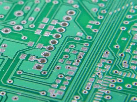
Effective PCB assembly relies on integrating automated processes, precision soldering, and rigorous quality control methods to ensure durable electronics. Modern PCBA workflows leverage robotic pick-and-place systems and reflow soldering to achieve micron-level accuracy, minimizing human error. Automated optical inspection (AOI) and X-ray testing further enhance reliability by detecting flaws like solder bridges or misaligned components.
To bolster durability, techniques such as conformal coating and thermal management solutions protect boards from environmental stressors. Optimizing PCB assembly also involves selecting materials with high glass transition temperatures (Tg) and implementing design-for-manufacturing (DFM) principles to reduce failure risks.
Moreover, advancements in laser soldering and 3D solder paste inspection (SPI) enable precise connections even for miniaturized components, critical for high-density designs. By aligning PCBA stages with real-time monitoring systems, manufacturers maintain consistency across production batches while accelerating time-to-market. These strategies collectively ensure robust circuit boards capable of meeting stringent industry standards.
Automated PCB Assembly Processes
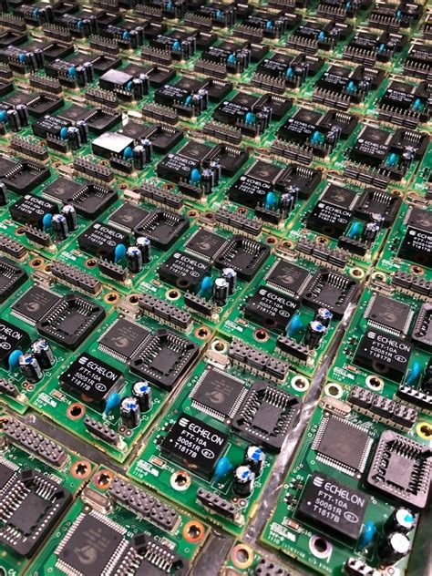
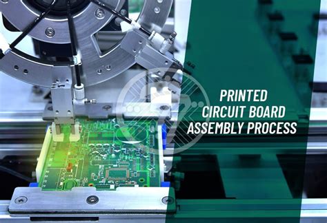
Modern electronics manufacturing relies heavily on automated PCB assembly workflows to ensure speed, accuracy, and repeatability. By integrating robotics and AI-driven systems, PCBA (printed circuit board assembly) lines minimize human error while handling complex tasks such as component placement, solder paste application, and thermal profiling. Surface-mount technology (SMT) machines, for instance, position microchips and resistors at rates exceeding 50,000 components per hour, achieving micron-level precision critical for high-density designs.
Tip: For optimal results, pair automated pick-and-place systems with inline optical inspection (AOI) tools to detect misaligned parts or soldering defects in real time.
Advanced conveyor systems synchronize with reflow ovens to maintain consistent thermal cycles, ensuring reliable solder joints across batches. Manufacturers also leverage machine learning algorithms to predict equipment maintenance needs, reducing downtime. A key advantage of automated PCB assembly is scalability—factories can rapidly reconfigure production lines for diverse product designs without compromising throughput.
"Automation isn’t just about speed; it’s about building a foundation for zero-defect manufacturing," notes a leading industry engineer.
By standardizing processes like stencil printing and component verification, PCBA automation strengthens traceability, a critical factor for industries requiring stringent compliance, such as aerospace or medical devices. This shift toward digitized workflows also supports seamless integration with enterprise resource planning (ERP) systems, enabling end-to-end supply chain visibility. As demand for miniaturized, high-performance electronics grows, these technologies will remain pivotal in balancing precision with mass-production demands.
Precision Soldering for Reliable PCBs
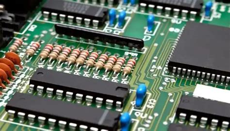
In modern PCB assembly, precision soldering forms the backbone of durable electronics, ensuring stable electrical connections even under demanding conditions. Advanced PCBA workflows leverage laser-guided soldering systems and nitrogen-reflow environments to minimize oxidation, achieving consistent solder joints for components as small as 01005 packages. Techniques like void-free soldering reduce thermal stress, critical for high-frequency or high-power applications where micro-cracks can compromise performance.
| Soldering Method | Key Advantage | Ideal Use Case |
|---|---|---|
| Reflow Soldering | Uniform heat distribution | High-density SMD components |
| Selective Soldering | Targeted application | Mixed-technology boards |
| Vapor Phase | Low thermal shock | Temperature-sensitive parts |
Automated PCB assembly lines integrate real-time thermal profiling to adjust soldering parameters dynamically, compensating for board warpage or component tolerances. Post-solder inspections using automated optical inspection (AOI) or X-ray imaging validate joint integrity, flagging issues like cold joints or tombstoning before final testing. By combining these methods, PCBA providers ensure solder reliability aligns with automotive or aerospace-grade standards, where failure rates must stay below 10 ppm. This focus on precision not only enhances product longevity but also streamlines downstream quality control processes.
Circuit Board Quality Control Methods
Effective quality assurance in PCB assembly relies on systematic inspection protocols that identify defects while ensuring compliance with industry standards. Automated optical inspection (AOI) systems are critical for detecting soldering anomalies, component misalignment, or missing parts by analyzing high-resolution images against predefined design parameters. Complementing AOI, X-ray inspection examines hidden connections in multilayer boards or PCBA units with ball grid array (BGA) components, revealing voids or cracks invisible to traditional methods.
For functional validation, in-circuit testing (ICT) verifies electrical performance by probing specific nodes to confirm voltage, resistance, and signal integrity. Environmental stress screening (ESS), including thermal cycling and vibration tests, further ensures boards withstand operational demands. Statistical process control (SPC) tools track production metrics—such as solder paste deposition accuracy—to preempt deviations before they escalate.
Integrating these methods into PCB assembly workflows reduces failure rates by up to 40%, as reported by leading electronics manufacturers. By aligning inspection stages with ISO 9001 and IPC-A-610 benchmarks, producers maintain consistency across high-volume PCBA outputs while minimizing rework costs. Advanced traceability systems, leveraging barcodes or RFID tags, further enhance defect resolution speed by linking test results to specific production batches.
Enhancing PCB Durability Through Techniques
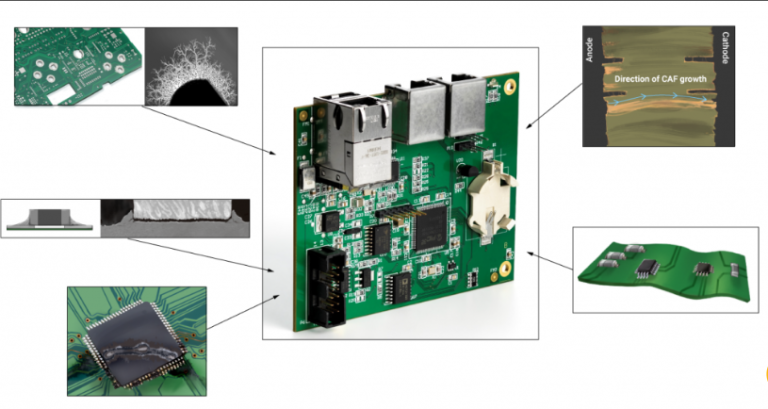
Durability in PCB assembly hinges on integrating material science, design optimization, and advanced manufacturing protocols. Selecting high-grade substrates like polyimide or FR-4 with halogen-free formulations ensures resistance to thermal stress and mechanical wear. To mitigate environmental degradation, PCBA workflows often employ conformal coating—a protective polymer layer that shields circuits from moisture, dust, and chemical exposure.
Automated optical inspection (AOI) systems further enhance reliability by identifying micro-cracks or soldering defects before final deployment. For applications demanding extreme ruggedness, techniques such as underfill encapsulation reinforce solder joints in ball grid array (BGA) components, reducing failure risks under vibration or thermal cycling. Additionally, thermal management strategies—like integrating copper-core vias or heat-dissipating pads—prevent overheating, a critical factor in extending PCB assembly lifespan.
Transitioning to lead-free solder alloys (e.g., SAC305) not only complies with environmental regulations but also improves joint integrity under prolonged operational stress. Combining these methods with rigorous accelerated life testing (ALT) ensures that PCBA outputs meet MIL-STD-883 standards for military-grade electronics or ISO-9001 benchmarks for industrial systems. By balancing precision manufacturing with proactive durability enhancements, engineers can deliver circuit boards capable of thriving in harsh operating environments.
Optimize Electronics Production With PCBA
Integrating PCB assembly (PCBA) into modern manufacturing workflows unlocks significant efficiency gains while ensuring consistent quality. By leveraging automated systems like pick-and-place machines and automated optical inspection (AOI), manufacturers reduce human error and accelerate throughput. These technologies enable precise component placement, critical for high-density boards used in advanced electronics. Thermal profiling during reflow soldering further ensures reliable connections, minimizing defects such as cold joints or tombstoning.
A streamlined PCBA process also incorporates real-time monitoring to detect anomalies early, preventing costly rework. For example, inline testing protocols validate solder joint integrity and electrical functionality before boards progress to final assembly. Additionally, adopting surface-mount technology (SMT) alongside mixed-technology assembly supports diverse design requirements, from consumer gadgets to industrial controllers.
To maximize durability, post-assembly treatments like conformal coating shield boards from environmental stressors. Pairing these techniques with design-for-manufacturing (DFM) principles ensures layouts align with assembly capabilities, reducing bottlenecks. By optimizing PCB assembly workflows, manufacturers achieve shorter lead times, higher yields, and electronics that meet rigorous reliability standards—key factors in today’s competitive markets.
Key Steps for Robust Circuit Board Assembly
Achieving reliable PCB assembly requires meticulous adherence to proven methodologies. The process begins with component selection, where high-grade materials compatible with the board’s design ensure longevity. Automated pick-and-place systems then position surface-mount devices (SMDs) with micron-level accuracy, minimizing placement errors that could compromise functionality.
Following this, precision soldering techniques—such as reflow or wave soldering—form secure electrical connections. Controlled temperature profiles prevent thermal stress, while solder paste inspection (SPI) systems verify joint integrity. For mixed-technology boards, selective soldering addresses through-hole components without affecting adjacent SMDs.
Quality assurance integrates automated optical inspection (AOI) and X-ray imaging to detect hidden defects like voids or misalignments. Environmental stress testing, including thermal cycling and vibration analysis, further validates durability under real-world conditions.
A critical phase in PCBA is conformal coating, which shields circuits from moisture, dust, and chemical exposure. Advanced robotic dispensers apply coatings uniformly, ensuring complete coverage without bridging contacts.
Finally, functional testing simulates operational scenarios to confirm performance metrics. By harmonizing these steps—from material selection to final validation—manufacturers deliver PCB assemblies that meet stringent reliability standards for industrial, automotive, and aerospace applications.
Innovative PCB Assembly Technologies
The evolution of PCB assembly technologies has redefined modern electronics manufacturing, enabling higher precision and scalability. Central to this progress is the integration of robotic pick-and-place systems, which streamline component placement with micron-level accuracy. These systems, combined with PCBA-optimized software, reduce human error while accelerating throughput—critical for high-volume production.
Another breakthrough lies in 3D solder jetting, a non-contact method that deposits solder paste with unparalleled consistency, even on high-density interconnect (HDI) designs. This technique minimizes void formation and enhances thermal reliability, particularly for devices operating in extreme environments. Additionally, laser-assisted soldering is gaining traction for its ability to target microscopic joints without affecting adjacent components, ensuring robust electrical connections.
To address quality challenges, manufacturers now deploy inline automated optical inspection (AOI) systems during PCB assembly. These systems perform real-time defect detection, such as misaligned components or insufficient solder, reducing post-production rework. Innovations like adaptive thermal profiling further optimize reflow oven settings, accounting for variations in board materials and component sizes.
By leveraging these advancements, PCBA workflows achieve tighter tolerances and improved repeatability—key factors in producing durable, high-performance electronics. As industry demands shift toward miniaturization and IoT integration, these technologies will remain pivotal in maintaining competitive and reliable manufacturing ecosystems.
Advanced Soldering Solutions for Electronics
Modern PCB assembly relies on precision soldering techniques to ensure electrical stability and long-term durability in electronic devices. Reflow soldering, a cornerstone of PCBA workflows, uses controlled heating profiles to melt solder paste uniformly across surface-mount components, minimizing defects like voiding or cold joints. For through-hole components, selective wave soldering targets specific areas, reducing thermal stress on sensitive parts. Advanced systems integrate nitrogen atmospheres during soldering to prevent oxidation, enhancing joint integrity in high-reliability applications such as aerospace or medical electronics.
Automated optical inspection (AOI) systems now complement these processes, scanning solder joints in real time to detect micron-level inconsistencies. Additionally, lead-free solder alloys align with global environmental standards while maintaining mechanical strength. For complex assemblies, laser soldering offers pinpoint accuracy for micro-components, critical in miniaturized designs. By optimizing temperature gradients and material selection, manufacturers achieve PCB assembly outcomes that withstand vibration, humidity, and thermal cycling—key factors in extending product lifespans. These innovations underscore how PCBA advancements directly translate to robust, field-ready electronics.
Conclusion
The evolution of PCB assembly methodologies underscores the critical role of precision and innovation in modern electronics manufacturing. By integrating automated processes and advanced PCBA workflows, manufacturers can achieve consistent quality while minimizing human error. Techniques such as laser-assisted soldering and 3D inspection systems not only enhance reliability but also extend the operational lifespan of circuit boards, aligning with demands for durable, high-performance devices.
As industries push toward miniaturization and higher complexity, the adoption of real-time monitoring and predictive analytics in PCB assembly lines becomes indispensable. These tools enable proactive identification of potential defects, ensuring adherence to stringent quality benchmarks. Moreover, the strategic use of lead-free soldering alloys and conformal coatings reinforces environmental compliance while safeguarding against mechanical stress and corrosion.
Ultimately, the synergy between PCBA automation and rigorous testing protocols creates a foundation for scalable, future-ready production. By prioritizing data-driven optimization and continuous process refinement, manufacturers can deliver electronics that meet both current standards and emerging technological challenges. This holistic approach solidifies PCB assembly as a cornerstone of robust, efficient electronics manufacturing.
Frequently Asked Questions
What distinguishes advanced PCB assembly from traditional methods?
Modern PCBA integrates automated optical inspection (AOI) and surface-mount technology (SMT), enhancing precision while reducing human error. These processes ensure consistent solder joint quality and faster production cycles.
How does automated soldering improve reliability in electronics?
Automated systems apply lead-free soldering alloys with micron-level accuracy, minimizing thermal stress on components. This reduces failure rates in high-frequency applications by maintaining stable electrical connections across PCB assemblies.
What quality control steps are critical for durable circuit boards?
Post-assembly tests like in-circuit testing (ICT) and X-ray inspection identify hidden defects, such as voids in solder joints. Combined with environmental stress screening, these methods validate PCBA performance under extreme conditions.
Can PCB durability be enhanced without increasing costs?
Yes. Techniques like conformal coating and edge plating protect against moisture and mechanical wear. Optimizing panelization designs during PCB assembly also reduces material waste, balancing durability and affordability.
Why is PCBA optimization vital for high-volume production?
Streamlined workflows using pick-and-place robots and real-time analytics cut downtime by 30–40%. This ensures scalable output while adhering to ISO 9001 standards, making PCB assembly viable for industries like automotive and aerospace.
Discover Tailored PCB Assembly Solutions
For specialized PCBA requirements, please click here to explore custom services that align with your project’s technical and compliance needs.