Advanced SMT Assembly Strategies for Reliable Electronics Manufacturing
Key Takeaways
Implementing advanced PCB assembly strategies requires a holistic approach that integrates precision engineering with process optimization. Modern SMT workflows leverage automated optical inspection (AOI) and 3D solder paste inspection (SPI) to reduce placement errors below 0.025mm, ensuring consistent alignment of microcomponents like 0201 passives. For PCBA applications, stencil design optimization paired with nitrogen-reflow soldering minimizes voiding rates to under 5%, significantly improving joint reliability.
"The shift toward data-driven process control in SMT assembly has reduced defect rates by 40% in high-density interconnect (HDI) boards," notes Dr. Elena Torres, a process engineering specialist at TechCircuit Solutions.
| Parameter | Traditional Approach | Advanced Strategy |
|---|---|---|
| Placement Accuracy | ±50μm | ±15μm |
| Thermal Cycling | 500 cycles | 1,200 cycles |
| Yield Rate | 92% | 98.5% |
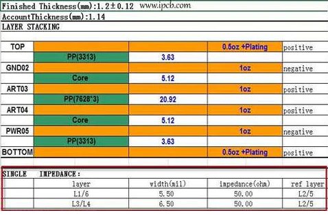
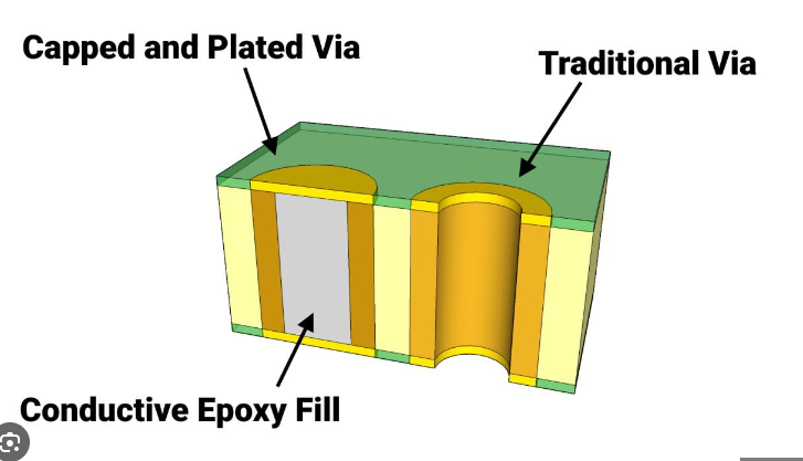
For thermal management, embedding copper-invar-copper (CIC) cores within multilayer PCBs reduces coefficient of thermal expansion (CTE) mismatch by 60%, critical for aerospace-grade assemblies. Additionally, adopting predictive maintenance algorithms in PCBA lines cuts unplanned downtime by 35% through real-time monitoring of pick-and-place nozzle wear.
Tip: When optimizing SMT workflows, prioritize closed-loop feedback systems that synchronize solder paste deposition rates with component placement speeds. This prevents tombstoning in ultra-fine-pitch QFN packages while maintaining throughput above 25,000 components per hour.
Optimizing SMT Assembly for Enhanced Precision
Achieving micrometer-level accuracy in PCB assembly requires a holistic approach that integrates advanced machinery, material science, and process controls. Central to this effort is the optimization of component placement systems, which leverage high-speed vision alignment and real-time feedback loops to minimize positional deviations. Modern PCBA lines employ precision stencil printing for solder paste deposition, ensuring uniform volume distribution critical for reliable solder joints. To further enhance repeatability, manufacturers are adopting closed-loop calibration systems that dynamically adjust parameters like nozzle pressure and feeder alignment during production.
Thermal profiling also plays a pivotal role, as even minor inconsistencies in reflow oven temperature gradients can lead to tombstoning or solder bridging. By combining infrared thermography with predictive algorithms, engineers fine-tune heating zones to accommodate varying component sizes and substrate materials. Additionally, the integration of inline 3D SPI (Solder Paste Inspection) systems enables immediate detection of paste height anomalies, reducing defects before components enter reflow. These strategies collectively ensure that PCB assembly processes meet the stringent tolerances demanded by aerospace, medical, and automotive applications, where nanosecond-level signal integrity hinges on flawless physical alignment.
Automated Soldering Techniques in Electronics Manufacturing
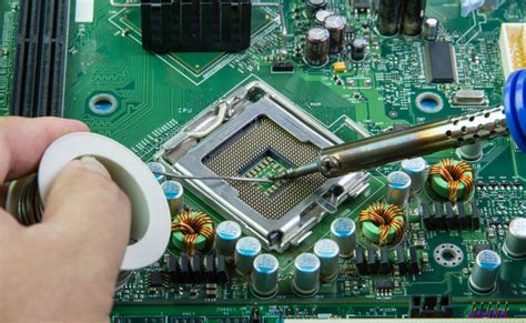
Modern PCB assembly relies heavily on automated soldering to ensure consistent quality and scalability in high-volume production. Reflow soldering remains a cornerstone of PCBA processes, leveraging precisely controlled thermal profiles to melt solder paste and form reliable electrical connections. Advanced systems now integrate real-time monitoring, adjusting parameters like temperature gradients and conveyor speed to accommodate variations in component density or board geometry. For through-hole components, wave soldering techniques are optimized using nitrogen-enriched environments to minimize oxidation, enhancing joint integrity.
The adoption of laser soldering has gained traction for applications requiring micron-level precision, particularly in mixed-technology assemblies combining surface-mount and fine-pitch components. Automated optical inspection (AOI) systems paired with X-ray imaging validate solder joint quality, flagging defects such as bridging or insufficient wetting before boards progress downstream. To address thermal stress in multilayer PCB assembly, manufacturers employ predictive algorithms that correlate solder profile settings with material coefficients of expansion, reducing warpage risks.
Transitioning seamlessly into component placement strategies, these soldering innovations underscore the importance of synchronized workflows in PCBA ecosystems. By harmonizing solder application accuracy with placement machinery tolerances, manufacturers achieve repeatable results while minimizing rework—a critical factor in maintaining yield rates across complex electronics assemblies.
Advanced Component Placement Strategies for SMT
Effective PCB assembly relies on precision in component placement, particularly in PCBA workflows where miniaturization and high-density layouts dominate. Modern pick-and-place systems leverage vision-guided robotics and machine learning algorithms to achieve micrometer-level accuracy, ensuring optimal alignment of components such as 0402 resistors or QFN packages. Advanced systems integrate real-time feedback loops to adjust for thermal expansion or board warpage, critical for maintaining solder joint integrity during reflow.
A key innovation lies in dynamic nozzle optimization, where machines automatically switch between nozzle sizes to handle components ranging from 0.25mm pitch BGAs to large electrolytic capacitors. This reduces downtime and improves throughput in high-mix production environments. Additionally, collision avoidance algorithms prevent misplacement by analyzing component height profiles and adjusting placement sequences dynamically.
For high-reliability applications, 3D AOI (Automated Optical Inspection) systems validate placement accuracy post-assembly, flagging issues like tombstoning or skewed orientations. Combining these strategies with design-for-manufacturability (DFM) principles ensures components are positioned to minimize thermal stress and signal interference, aligning with broader goals of process optimization. By integrating these techniques, manufacturers enhance yield rates while meeting stringent quality benchmarks in PCB assembly workflows.
Thermal Management Solutions for Reliable PCBs
Effective thermal management is critical in PCB assembly to ensure long-term reliability, particularly in high-density or power-intensive applications. Modern PCBA designs increasingly incorporate advanced techniques such as thermal vias, copper pours, and heat sinks to dissipate excess energy efficiently. For instance, thermally conductive materials like aluminum substrates or ceramic-filled laminates are strategically integrated into multilayer boards to optimize heat distribution.
Automated infrared inspection systems now enable real-time monitoring of temperature gradients during reflow soldering, identifying hotspots that could compromise component integrity. Engineers also leverage simulation tools to model airflow patterns and predict thermal stress before physical prototyping, reducing iterative costs. In high-power PCB assembly, the use of thermal interface materials (TIMs) between components and heatsinks ensures minimal thermal resistance, enhancing overall system stability.
Moreover, design-for-manufacturing (DFM) principles emphasize balanced trace routing and component spacing to prevent localized overheating. By aligning these strategies with PCBA process controls—such as optimized solder paste application and precise oven profiling—manufacturers achieve consistent thermal performance across production batches. This systematic approach not only extends product lifespans but also aligns with industry demands for miniaturized, high-reliability electronics.
Quality Control Methods in SMT Assembly Processes
Effective quality control in PCB assembly relies on a combination of automated inspection systems and data-driven process monitoring. Modern PCBA production lines integrate real-time optical inspection (AOI) systems to detect soldering defects, component misalignment, or tombstoning at micron-level resolutions. Advanced X-ray imaging further examines hidden connections in high-density interconnects (HDIs), ensuring BGA and QFN packages meet joint integrity standards.
Statistical process control (SPC) software analyzes solder paste deposition metrics, reflow oven thermal profiles, and placement machine accuracy, creating feedback loops that continuously refine manufacturing parameters. For mission-critical applications, environmental stress screening (ESS) subjects assembled boards to thermal cycling and vibration tests, validating reliability under extreme conditions.
To maintain traceability, manufacturers implement blockchain-enabled documentation systems that track component lot numbers, machine calibration records, and test results across the SMT assembly workflow. This approach not only aligns with ISO 9001 standards but also enables rapid root-cause analysis when yield anomalies occur. By integrating these methods, PCBA providers achieve first-pass yield rates exceeding 99.4% while meeting stringent automotive and medical device compliance requirements.

Boosting Production Yield with SMT Process Optimization
Optimizing SMT assembly processes is central to maximizing production yield in modern PCBA workflows. By refining solder paste application, reflow profiling, and inspection protocols, manufacturers can reduce defects like tombstoning or solder bridging. Key strategies include implementing automated optical inspection (AOI) systems to detect misaligned components early and leveraging real-time process monitoring to adjust parameters dynamically. For instance, precise control of reflow oven temperature gradients ensures consistent solder joint formation, directly impacting the reliability of PCB assembly outcomes.
Advanced stencil design plays a pivotal role in minimizing solder paste waste and improving deposition accuracy. Combining laser-cut stencils with nano-coated surfaces enhances release efficiency, particularly for fine-pitch components. Additionally, integrating statistical process control (SPC) tools enables data-driven adjustments, reducing variability across batches. Manufacturers adopting closed-loop feedback systems report yield improvements of 15–20%, as anomalies are flagged and corrected before escalating into costly rework.
To further align with high-volume demands, optimizing pick-and-place machine programming ensures faster cycle times without compromising placement precision. Pairing this with predictive maintenance schedules for SMT equipment minimizes downtime, sustaining throughput. By harmonizing these techniques, PCBA lines achieve not only higher yields but also long-term cost efficiencies, reinforcing the critical link between process refinement and manufacturing success.
Precision-Driven SMT Assembly for High-Reliability Electronics
Achieving high-reliability electronics demands meticulous attention to detail in PCB assembly processes, particularly when integrating surface-mount technology (SMT). Precision-driven PCBA workflows rely on advanced tools like automated optical inspection (AOI) and X-ray inspection systems to detect micron-level misalignments or solder joint defects, ensuring compliance with stringent industry standards such as IPC-A-610. Modern SMT assembly leverages high-speed component placement systems equipped with vision-guided robotics, enabling accuracies within ±25 microns for even the smallest 0201 or 01005 packages.
Critical to this precision is the integration of real-time process monitoring, which tracks variables like solder paste deposition volume and reflow oven temperature gradients. These systems adjust parameters dynamically, minimizing voids or tombstoning in PCB assembly lines. For thermally sensitive components, engineers employ predictive thermal modeling to optimize reflow profiles, balancing heat distribution across multilayer boards. Such strategies are vital in aerospace or medical PCBA applications, where component failure is not an option.
By coupling these technologies with AI-driven analytics, manufacturers achieve traceability from placement to final testing, closing quality loops in SMT assembly workflows. This holistic approach ensures that precision isn’t just a metric—it’s a repeatable outcome for mission-critical electronics.
Conclusion
The evolution of SMT assembly has redefined modern PCB assembly by integrating precision, automation, and data-driven decision-making. As high-reliability electronics demand tighter tolerances and faster production cycles, adopting advanced PCBA strategies becomes non-negotiable. Techniques like automated soldering and AI-powered component placement systems ensure consistent quality while minimizing human error, directly contributing to enhanced thermal management and long-term device reliability.
By prioritizing real-time process optimization and rigorous quality control protocols, manufacturers can address challenges such as microvoiding, solder bridging, and thermal stress. The strategic implementation of SMT process optimization not only elevates yield rates but also enables scalable solutions for complex, miniaturized designs. As the industry shifts toward smart manufacturing ecosystems, the synergy between advanced PCB assembly technologies and IoT-enabled monitoring systems will further solidify PCBA as the backbone of next-generation electronics. Moving forward, continuous innovation in material science and machine learning algorithms will remain pivotal in maintaining the delicate balance between production speed, cost-efficiency, and zero-defect manufacturing standards.
Frequently Asked Questions
What distinguishes SMT assembly from traditional through-hole methods in PCB assembly?
SMT (Surface Mount Technology) enables smaller component placement, higher circuit density, and faster production compared to through-hole techniques. This method reduces manual intervention, improving consistency in PCBA workflows.
How does automated soldering enhance reliability in electronics manufacturing?
Automated systems like reflow ovens ensure precise temperature control, minimizing defects like cold joints. Pairing this with AOI (Automated Optical Inspection) guarantees solder joint integrity, critical for high-reliability PCB assembly.
What strategies prevent thermal stress during SMT assembly?
Implementing thermal profiling and using materials with matched CTE (Coefficient of Thermal Expansion) reduces warping. Advanced PCBAs often integrate heat sinks or thermal vias for optimal dissipation.
Why is component placement accuracy vital for production yield?
High-precision pick-and-place machines achieve micron-level alignment, avoiding misregistration. This is especially crucial for fine-pitch components in modern PCB assembly, where errors directly impact functional reliability.
How do quality control systems adapt to miniaturized SMT components?
Combining X-ray inspection and ICT (In-Circuit Testing) identifies hidden flaws in dense PCBAs. Machine learning algorithms further refine defect detection, aligning with Industry 4.0 standards.
Ready to Optimize Your SMT Assembly Process?
For tailored solutions in PCB assembly and PCBA workflows, please click here to consult our engineering team.