Advanced Techniques for PCB Signal Loop Design
Introduction
Printed Circuit Board (PCB) design has become increasingly complex as electronic devices demand higher speeds, greater functionality, and smaller form factors. Among the most critical aspects of PCB design is proper signal loop management, which directly impacts signal integrity, electromagnetic compatibility (EMC), and overall system performance. This article explores advanced techniques for mastering PCB signal loops, offering professional insights that go beyond basic design principles.
Understanding Signal Loops
The Nature of Current Flow
A fundamental principle often overlooked is that all electrical current flows in loops. While designers typically focus on the intentional signal path from transmitter to receiver, the return current path is equally important. At DC and low frequencies, current follows the path of least resistance, while at high frequencies, it follows the path of least inductance—typically directly beneath the signal trace in the reference plane.
Loop Area Considerations
The area enclosed by the outgoing and returning current paths creates what we call the “loop area.” This area is crucial because:
- Larger loop areas generate more electromagnetic interference (EMI)
- Larger loops have higher inductance, affecting signal quality
- They act as more efficient antennas for both emitting and receiving noise
Advanced Loop Control Techniques
1. Proper Reference Plane Management
Continuous Planes vs. Split Planes
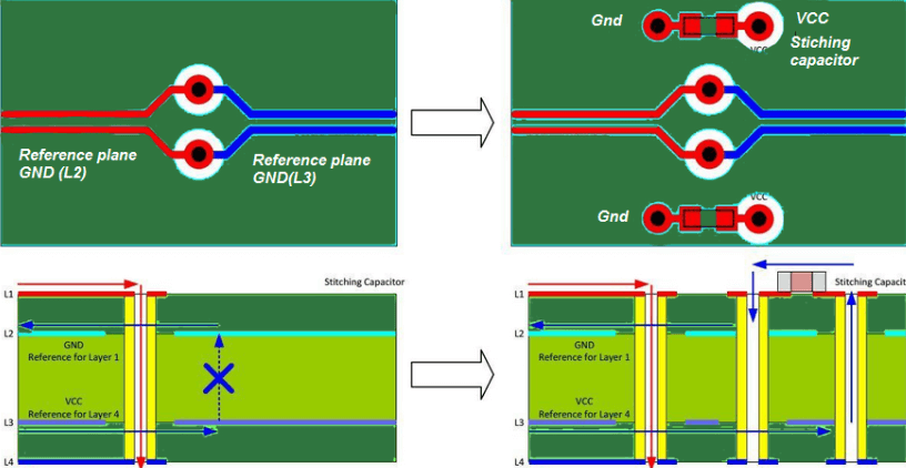
Maintain continuous reference planes whenever possible, especially for high-speed signals. Split planes can force return currents to take long detours, dramatically increasing loop area. When splits are unavoidable:
- Place bypass capacitors near where signals cross plane splits
- Route critical signals to avoid crossing splits
- Consider the return current path when placing plane splits
Plane Proximity
Place signal layers adjacent to solid reference planes. The closer the signal layer is to its reference plane, the smaller the loop area becomes. For critical signals:
- Use thinner dielectric materials between signal and plane layers
- Avoid routing over plane discontinuities like slots or cutouts
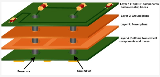
2. Strategic Via Placement and Design
Return Vias for Layer Transitions
When a signal changes layers, its return current must also find a path between reference planes. Best practices include:
- Placing return vias immediately adjacent to signal vias (within 50 mils)
- Using multiple return vias for very high-speed signals
- Ensuring reference planes at different potentials are properly decoupled
Via Stitching
For shielding and containment:
- Create via fences around sensitive signals or noise sources
- Use ground vias to connect split reference planes at edges
- Implement via stitching along the perimeter of boards
3. Differential Pair Optimization
Maintaining Pair Integrity
Proper differential signaling relies on careful loop control:
- Keep trace lengths matched (phase matched) to within 5 mils
- Maintain consistent spacing between pair members
- Route pairs over continuous reference planes
Common Mode Control
Even differential signals can create problematic loops through common mode currents:
- Use common mode chokes when needed
- Ensure symmetrical termination
- Maintain balance in the physical layout
4. Power Delivery Network (PDN) as Part of the Loop
Decoupling Capacitor Placement
The power delivery network forms part of many signal loops:
- Place decoupling capacitors as close as possible to IC power pins
- Use multiple capacitor values in parallel
- Consider the loop formed by capacitor placement
Plane Capacitance
Maximize inherent plane capacitance:
- Use thin dielectric between power and ground planes
- Consider interdigitated power/ground planes in dense designs
Specialized Techniques for Challenging Scenarios
Mixed-Signal Design
Strategic Grounding Approaches
For mixed-signal systems:
- Implement “moat and bridge” techniques where appropriate
- Use split planes only when necessary, with careful attention to return paths
- Consider single-point grounding for very low frequency analog
Digital Isolation
When complete isolation is needed:
- Use transformers or opto-isolators with proper barrier design
- Ensure sufficient clearance and creepage distances
- Pay attention to inter-winding capacitance in isolation components
High-Speed Serial Links
Pre-Emphasis and Equalization
For multi-gigabit links:
- Implement transmitter pre-emphasis to compensate for losses
- Use receiver equalization to improve signal integrity
- Simulate the entire channel including connectors
Backdrilling for Stubs
In high-speed designs:
- Specify backdrilling for long via stubs
- Consider microvias or HDI techniques
- Model via structures in your simulations
Verification and Analysis Techniques
3D Field Solver Simulations
Advanced simulation tools can:
- Model complex current paths in three dimensions
- Identify unexpected loop areas
- Predict EMI radiation patterns
Time Domain Reflectometry (TDR)
TDR measurements help:
- Identify impedance discontinuities
- Locate unexpected return path discontinuities
- Verify transmission line quality
Near-Field Scanning
Practical EMI assessment:
- Identify “hot spots” of radiation
- Verify effectiveness of containment strategies
- Correlate simulation with real-world performance
Common Pitfalls and How to Avoid Them
1. Ignoring Return Path Discontinuities
Symptoms:
- Unexpected resonances
- Increased EMI at specific frequencies
- Signal integrity issues
Solutions:
- Carefully analyze return paths for all signals
- Provide alternative paths at discontinuities
- Use simulation to identify problem areas
2. Overlooking Inter-layer Coupling
Symptoms:
- Crosstalk between unrelated signals
- Noise coupling into sensitive circuits
- Unexpected common mode currents
Solutions:
- Maintain proper spacing between unrelated signals
- Use guard traces or ground shielding where needed
- Consider orthogonal routing on adjacent layers
3. Neglecting Edge Effects
Symptoms:
- Increased radiation from board edges
- Ground bounce issues
- Impedance variations near edges
Solutions:
- Implement proper board edge termination
- Use via stitching along edges
- Maintain adequate keep-out areas
Future Trends in Loop Control
Embedded Passives
Integration of decoupling within the PCB substrate:
- Reduces loop inductance
- Saves board space
- Improves high-frequency performance
3D Printed Electronics
Additive manufacturing techniques may enable:
- Novel current path geometries
- Integrated shielding structures
- Customized dielectric properties
AI-Assisted Layout
Machine learning applications could:
- Automatically optimize return paths
- Predict and prevent loop issues
- Suggest optimal component placement
Conclusion
Mastering PCB signal loop techniques requires both theoretical understanding and practical experience. By implementing these advanced methods—proper reference plane management, strategic via placement, differential pair optimization, and comprehensive PDN design—engineers can significantly improve signal integrity and EMC performance. Remember that every design presents unique challenges, and the most effective solutions often combine multiple techniques tailored to the specific application. Continuous learning through simulation, measurement, and analysis remains essential for staying ahead in the ever-evolving field of PCB design.
As digital systems continue to push speed and density boundaries, the principles of good loop control become even more critical. By applying these advanced techniques, designers can create robust, high-performance PCBs that meet stringent requirements while minimizing costly redesigns and compliance issues.


