Advantages and Strategies of Using Differential Signal Lines in PCB Design
Differential signal pairs that are routed very close to each other will also be tightly coupled to each other. This mutual coupling will reduce EMI emissions. The main disadvantage of differential signal lines is that they increase the area of the PCB. This article introduces the routing strategies of using differential signal lines in PCB design.
As we all know, signals have the characteristic of being transmitted along signal lines or under PCB lines. Even though we may not be familiar with single-ended mode routing strategies, the term single-ended distinguishes this transmission characteristic of signals from differential mode and common mode signal transmission methods, which are usually more complicated.
Differential and Common Mode
Differential signals are transmitted through a pair of signal lines. One signal line transmits the signal we usually understand; the other signal line transmits a signal of equal value but opposite direction (at least in theory).
There was little difference between differential and single-ended modes when they first appeared, because all signals have loops.
Single-ended mode signals usually return through a zero voltage circuit (or ground). Each signal in the differential signal must return through the ground circuit. Since each signal pair is actually equal and opposite, the return circuits simply cancel each other out, so there is no differential signal return component on the zero voltage or ground circuit.
Common mode refers to the signal appearing on both signal lines of a (differential) signal line pair, or on a single-ended signal line and ground at the same time. Understanding this concept is not intuitive, because it is difficult to imagine how such a signal is generated. This is mainly because we do not usually generate common mode signals. Most common mode signals are noise signals generated in the circuit according to hypothetical situations or coupled in by adjacent or external signal sources. Common mode signals are almost always “harmful”, and many design rules are designed to prevent common mode signals from appearing.
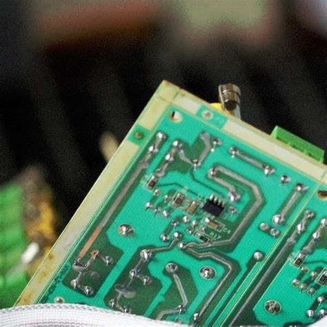
Routing of differential signal lines
Usually (of course there are some exceptions) differential signals are also high-speed signals, so high-speed design rules usually apply to the routing of differential signals, especially when designing signal lines such as transmission lines1. This means that we must design the routing of signal lines very carefully to ensure that the characteristic impedance of the signal line is continuous and constant along the signal line.
During the layout and routing of differential pairs, we hope that the two PCB lines in the differential pair are exactly the same. This means that in practical applications, we should make every effort to ensure that the PCB lines in the differential pair have exactly the same impedance and the wiring length is exactly the same.
Differential PCB lines are usually always routed in pairs, and the distance between them remains constant at any position along the direction of the line pair. Usually, the layout and routing of differential pairs are always as close as possible.
Advantages of differential signals
Single-ended signals are usually always referenced to a certain “reference” level. This “reference” level may be a positive voltage or a ground voltage, a threshold voltage of a device, or another signal somewhere else. On the other hand, differential signals always refer to the other side of the differential pair.
That is, if the voltage on one signal line (+ signal) is higher than the voltage on the other signal line (- signal), we get one logic state; if the former is lower than the latter, we get another logic state, see Figure 1.
Differential signals have the following advantages:
1. Timing is precisely defined, because it is easier to control the intersection of the signal line pairs than to control the absolute voltage value of the signal relative to a reference level. This is also a reason for accurately implementing equal-length routing of differential line pairs. If the signals do not reach the other end of the differential line pair at the same time, then any timing control that the source can provide will be greatly reduced. In addition, if the signals at the far end of the differential line pair are not strictly equal in value but reversed, common-mode noise will appear, which will cause problems with signal timing and EMI.
2. Because differential signals do not refer to any signals other than themselves and the timing of signal intersections can be more strictly controlled, differential circuits can usually operate at higher speeds than conventional single-ended signal circuits.
Since differential circuits operate on the difference between the signals on two lines (whose signals are equal but opposite), the resulting signal is twice as large as any single-ended signal compared to the surrounding noise. Therefore, all other things being equal, differential signals always have a higher signal-to-noise ratio and therefore provide higher performance.
Differential circuits are very sensitive to differences between the signal levels on the differential pair. However, they are not sensitive to the absolute voltage values on the differential lines relative to some other reference (especially ground). Differential circuits are relatively insensitive to problems such as ground bounce and other noise signals that may exist on the power and ground planes, while common-mode signals appear exactly the same on each signal line.
Differential signals are also somewhat immune to EMI and crosstalk coupling between signals. If a pair of differential signal lines are routed very closely, any externally coupled noise will couple to each signal line in the pair to the same degree. The coupled noise is therefore “common-mode” noise, and differential signal circuits are perfectly immune to this. If the pairs are twisted together (such as twisted pair), the signal lines will be more immune to coupled noise. Since it is not easy to twist differential signals on a PCB, it is a good idea to route them as close together as possible.
Differential signal pairs that are routed very close to each other will also be tightly coupled to each other. This mutual coupling will reduce EMI emissions, especially compared to single-ended PCB signal lines. You can imagine that the radiation from each signal line in a differential signal is equal in magnitude and opposite in direction, so they will cancel each other out, just like the signal in a twisted pair. The closer the differential signals are routed, the stronger the coupling between them, and the less EMI radiation will be.
The main disadvantage of differential circuits is the increase in PCB lines. Therefore, if the advantages of differential signals cannot be utilized during the application process, it is not worth increasing the PCB area. However, if the designed circuit has significant improvements in performance, then the cost of increased routing area is worth it.
This article summarizes
Differential signal lines will couple with each other. This coupling affects the apparent impedance of the signal line, so a termination strategy must be used (see Note 2 for discussion and calculation of differential impedance). Calculating differential impedance is difficult, and National Semiconductor provides some references in this area. Polar Instruments also provides a stand-alone differential impedance calculator that can calculate many different differential signal structures


