An Approach to High-Power PCB Thermal Management
The entire power electronics industry, including RF applications and systems involving high-speed signals, is moving toward solutions that provide increasingly complex functionality in increasingly smaller spaces. Designers face increasingly demanding challenges in meeting system size, weight, and power requirements, which includes effective thermal management, starting with the design of the printed circuit board.
High integration density active power devices, such as MOSFET transistors, can dissipate a lot of heat, requiring a PCB that can transfer heat from the hottest components to a ground plane or heat sink surface and operate as efficiently as possible. Thermal stress is one of the leading causes of power device failure, as it can lead to performance degradation and can even cause system failure or malfunction. The rapid growth of device power density and the continuous increase in frequency are the main causes of overheating of electronic components. The increasing use of semiconductors with reduced power losses and better thermal conductivity, such as wide bandgap materials, is not sufficient in itself to eliminate the need for effective thermal management.
The junction temperature of current silicon-based power devices is between approximately 125°C and 200°C. However, it is always preferred to operate the device below this limit, as this can cause rapid device degradation and shorten its remaining life. In fact, it is estimated that a 20°C increase in operating temperature due to improper thermal management can reduce the remaining life of a component by up to 50%.

Layout Approach
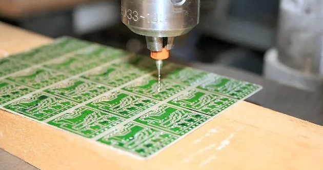
The common approach to thermal management in many projects is to use a substrate with standard flame retardant rating 4 (FR-4), an inexpensive and easy to process material, and focus on thermal optimization of the circuit layout.
The main measures adopted involve providing additional copper surface, using thicker traces, and inserting thermal vias under the components that generate the most heat.
A more radical technique, capable of dissipating more heat, involves inserting or applying a real copper block to the outermost layer of the PCB, usually in the shape of a coin (hence the name “copper coin”). The copper coin is processed separately and then soldered or attached directly to the PCB, or it can be inserted into the inner layer and connected to the outer layer through thermal vias.
The thermal conductivity of copper is 380 W/mK, while aluminum is 225 W/mK and FR-4 is 0.3 W/mK.
Copper is a relatively cheap metal that has been widely used in PCB manufacturing; therefore, it is an ideal choice for making copper coins, heat dissipation vias and ground planes, all solutions that are able to improve heat dissipation.
The correct positioning of active components on the board is a key factor in preventing the formation of hot spots, thus ensuring that the heat is distributed as evenly as possible throughout the board.
In this regard, the active components should be distributed in no particular order around the PCB to avoid the formation of hot spots in specific areas. However, it is best to avoid placing active components that generate a lot of heat near the edge of the board. Instead, they should be placed as close to the center of the board as possible, which is conducive to even heat distribution. If a high-power device is mounted near the edge of the board, heat will accumulate at the edge, increasing the local temperature.
On the other hand, if it is placed near the center of the board, the heat will be dissipated on all sides of the surface, reducing the temperature and making it easier to dissipate heat. Power devices should not be placed close to sensitive components and should be properly spaced from each other.
The measures taken at the layout level can be further improved by adopting active or passive cooling systems, such as heat sinks or fans, whose function is to remove heat from active components instead of directly dissipating heat into the board. In general, designers must find the right compromise between different thermal management strategies based on the requirements of a specific application and the available budget.

PCB Substrate Selection
Due to its low thermal conductivity (between 0.2 and 0.5 W/mK), FR-4 is generally not suitable for applications that need to dissipate a lot of heat. The amount of heat that can be generated in high-power circuits is considerable, and these systems often operate in harsh environments and extreme temperatures. Using alternative substrate materials with higher thermal conductivity may be a better choice than using traditional FR-4.
For example, ceramic materials offer significant advantages for thermal management of high-power PCBs.
In addition to improved thermal conductivity, these materials also have excellent mechanical properties that help compensate for stresses accumulated during repeated thermal cycling. In addition, ceramic materials have low dielectric losses at frequencies up to 10 GHz. For higher frequencies, there is always the option of hybrid materials (such as PTFE), which offer equally low losses with a modest reduction in thermal conductivity.
The higher the thermal conductivity of a material, the faster the heat transfer.
Therefore, metals such as aluminum offer an excellent solution for transferring heat away from components, in addition to being lighter than ceramics. Aluminum, in particular, is an excellent conductor, has excellent durability, is recyclable, and is non-toxic. Due to their high thermal conductivity, metal layers help transfer heat quickly throughout the board. Some manufacturers also offer metal-clad PCBs, where both outer layers are metal-clad, typically aluminum or galvanized copper. Aluminum is the best choice from a cost-per-weight perspective, while copper has a higher thermal conductivity. Aluminum is widely used to build PCBs that support high-power LEDs,
Even silver, due to its approximately 5% higher thermal conductivity than copper, can be used to make tracks, vias, pads, and metal layers.
Additionally, if the board is used in a humid environment where toxic gases are present, using a silver finish on exposed copper traces and pads will help prevent corrosion, a typical threat found in these environments.
Metal PCBs, also known as Insulated Metal Substrates (IMS), can be laminated directly into PCBs to form boards with FR-4 substrates and metal cores, in single- and double-layer technologies with deep controlled routing for transferring heat from onboard components to less critical areas. In IMS PCBs, a thin layer of thermally conductive but electrically insulating dielectric is laminated between the metal base and copper foil. The copper foil is etched into the desired circuit pattern, and the metal base absorbs heat from this circuit through the thin dielectric.
The main advantages offered by IMS PCBs are as follows:
Significantly higher heat dissipation than standard FR-4 construction.
· The thermal conductivity of the dielectric is typically 5 to 10 times that of ordinary epoxy glass.
· Heat transfer is much more efficient than with conventional PCBs.
In addition to LED technology (illuminated signs, displays, and lighting), IMS boards are widely used in the automotive industry (headlights, engine controls, and power steering), power electronics (DC power supplies, inverters, and engine controls), switches, and semiconductor relays.