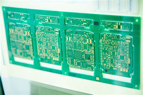
Analog technologies pcb manufacturing unit
Evolution Of Analog Technologies In PCB Manufacturing
The evolution of analog technologies in printed circuit board (PCB) manufacturing has been a fascinating journey marked by significant advancements and innovations. Initially, the development of PCBs was driven by the need to create more efficient and compact electronic devices.
As technology progressed, the demand for more sophisticated and reliable PCBs increased, leading to the integration of analog technologies that have transformed the manufacturing process.
In the early stages, PCB manufacturing was a labor-intensive process, relying heavily on manual techniques.
However, the introduction of analog technologies brought about a paradigm shift. These technologies enabled the automation of various manufacturing processes, significantly enhancing precision and efficiency. For instance, the use of analog signal processing in the design and testing phases allowed for more accurate simulations and analyses, ensuring that the final product met the desired specifications.
Moreover, analog technologies have played a crucial role in improving the quality and performance of PCBs.
By incorporating analog components, manufacturers have been able to achieve better signal integrity and reduce electromagnetic interference, which are critical factors in the functionality of electronic devices. This has been particularly important in applications where high-frequency signals are involved, such as in telecommunications and computing.
As the complexity of electronic devices increased, so did the need for more advanced PCB designs.
Analog technologies facilitated the development of multi-layer PCBs, which allowed for more components to be integrated into a single board. This not only saved space but also improved the overall performance of the device. The ability to stack multiple layers of circuitry has been instrumental in the miniaturization of electronic devices, a trend that continues to this day.
Furthermore, the integration of analog technologies in PCB manufacturing has led to significant cost reductions.
Automated processes have minimized the need for manual labor, reducing production costs and increasing output. Additionally, the precision offered by analog technologies has decreased the likelihood of errors, leading to less waste and rework. This has made PCB manufacturing more sustainable and economically viable, allowing manufacturers to offer competitive pricing while maintaining high-quality standards.
In recent years, the evolution of analog technologies in PCB manufacturing has been further accelerated by the advent of new materials and techniques.
For example, the use of advanced substrates and conductive inks has enabled the production of flexible and lightweight PCBs, opening up new possibilities for innovative designs and applications. These advancements have been particularly beneficial in industries such as wearable technology and medical devices, where flexibility and weight are critical considerations.
Looking ahead, the continued evolution of analog technologies in PCB manufacturing is expected to drive further innovations.
As the demand for more complex and efficient electronic devices grows, manufacturers will need to explore new ways to integrate analog technologies into their processes. This may involve the development of novel materials, the adoption of cutting-edge manufacturing techniques, or the implementation of advanced design tools.
In conclusion, the evolution of analog technologies in PCB manufacturing has been a key factor in the advancement of electronic devices. By enhancing precision, improving performance, and reducing costs, these technologies have transformed the industry and paved the way for future innovations. As technology continues to evolve, the role of analog technologies in PCB manufacturing will undoubtedly remain crucial, driving further progress and enabling the creation of increasingly sophisticated electronic devices.
Key Components In Analog PCB Design And Production
In the realm of electronics, the design and production of printed circuit boards (PCBs) for analog technologies play a crucial role in ensuring the functionality and reliability of various devices. Analog PCBs are integral to a wide range of applications, from audio equipment to communication systems, and their design requires a meticulous approach to accommodate the unique challenges posed by analog signals. Understanding the key components involved in analog PCB design and production is essential for engineers and manufacturers aiming to achieve optimal performance and efficiency.
To begin with, the selection of materials is a fundamental aspect of analog PCB design.
The choice of substrate material can significantly impact the electrical performance of the board. Common materials include FR-4, a glass-reinforced epoxy laminate, which is widely used due to its balance of cost and performance. However, for high-frequency applications, materials such as Rogers or Teflon may be preferred due to their superior dielectric properties. The material choice affects parameters like signal integrity and thermal management, which are critical in analog applications.
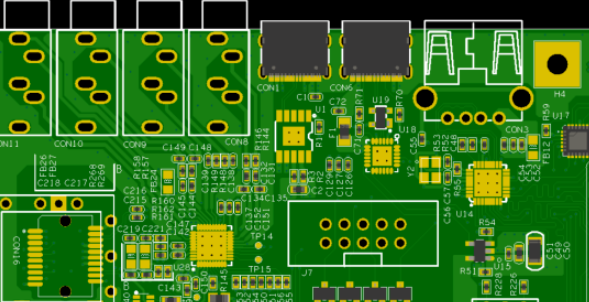
Transitioning to the layout design, the placement of components on an analog PCB requires careful consideration to minimize interference and signal loss.
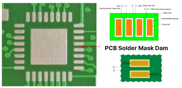
Components such as resistors, capacitors, and inductors must be strategically positioned to ensure that the analog signals are transmitted with minimal distortion. Additionally, the routing of traces is a vital component of the design process. Traces must be kept as short as possible to reduce parasitic inductance and capacitance, which can degrade signal quality. Moreover, the use of ground planes is essential in providing a return path for signals and reducing electromagnetic interference (EMI).
Another key component in analog PCB design is the power supply design.
Analog circuits are often sensitive to power supply noise, which can introduce unwanted variations in signal processing. Therefore, designing a stable and clean power supply is paramount. This involves the use of decoupling capacitors placed close to the power pins of integrated circuits to filter out high-frequency noise. Furthermore, the implementation of voltage regulators can help maintain a consistent voltage level, ensuring the reliable operation of analog components.
In addition to these design considerations, the production process of analog PCBs also demands precision and attention to detail.
The manufacturing process typically involves several stages, including etching, drilling, and soldering. Each stage must be executed with accuracy to prevent defects that could compromise the board’s performance. For instance, the etching process must ensure that the copper traces are precisely formed to maintain the intended electrical characteristics. Similarly, the drilling process must be conducted with precision to accommodate the placement of through-hole components.
Moreover, quality control is an indispensable part of the production process.
Rigorous testing and inspection are necessary to identify any defects or inconsistencies in the PCBs. Techniques such as automated optical inspection (AOI) and X-ray inspection are commonly employed to detect issues such as misaligned components or soldering defects. By ensuring that each PCB meets the required standards, manufacturers can guarantee the reliability and longevity of the final product.
In conclusion, the design and production of analog PCBs involve a complex interplay of material selection, layout design, power supply considerations, and meticulous manufacturing processes. Each component plays a vital role in ensuring that the final product meets the stringent requirements of analog applications. By understanding and addressing these key components, engineers and manufacturers can create PCBs that deliver exceptional performance and reliability in a wide array of analog technologies.

Challenges In Analog PCB Manufacturing And Solutions
Analog technologies have long been a cornerstone of electronic systems, providing the essential interface between the digital world and the physical environment. However, the manufacturing of printed circuit boards (PCBs) for analog applications presents a unique set of challenges that require careful consideration and innovative solutions.
One of the primary challenges in analog PCB manufacturing is maintaining signal integrity.
Analog signals are inherently susceptible to noise and interference, which can significantly degrade performance. This issue is exacerbated by the increasing demand for miniaturization, which necessitates tighter component placement and more complex routing. To address this, manufacturers must employ meticulous design practices, such as optimizing trace widths and spacing, and implementing effective grounding techniques to minimize electromagnetic interference.
Another significant challenge is the thermal management of analog PCBs.
Analog components, such as power amplifiers and voltage regulators, often generate substantial heat during operation. If not properly managed, this heat can lead to component failure and reduced reliability. Advanced thermal management solutions, such as the use of thermal vias, heat sinks, and thermal interface materials, are essential to dissipate heat effectively. Additionally, manufacturers are increasingly turning to simulation tools to predict thermal behavior and optimize designs before production.
Material selection also plays a crucial role in the manufacturing of analog PCBs.
The choice of substrate material can impact the board’s electrical performance, thermal characteristics, and mechanical stability. High-frequency analog applications, for instance, require materials with low dielectric loss to ensure signal fidelity. Manufacturers must carefully evaluate material properties and consider trade-offs between performance, cost, and manufacturability. Collaborating with material suppliers to develop custom solutions can also be beneficial in meeting specific application requirements.
Furthermore, the complexity of analog circuits often necessitates multi-layer PCB designs, which introduce additional manufacturing challenges.
Ensuring precise layer alignment and reliable inter-layer connections is critical to the board’s functionality. Advanced fabrication techniques, such as laser drilling for microvias and automated optical inspection, are employed to achieve the necessary precision and quality control. Moreover, manufacturers must continuously invest in state-of-the-art equipment and processes to keep pace with evolving industry standards and customer expectations.
In addition to technical challenges, analog PCB manufacturing is also subject to stringent regulatory requirements.
Compliance with standards such as RoHS (Restriction of Hazardous Substances) and REACH (Registration, Evaluation, Authorization, and Restriction of Chemicals) is mandatory, necessitating careful selection of materials and processes. Manufacturers must implement robust quality management systems to ensure compliance and traceability throughout the production process. This often involves extensive documentation and testing to verify that products meet all applicable standards.
Despite these challenges, the demand for analog PCBs continues to grow, driven by applications in telecommunications, automotive, medical devices, and consumer electronics.
To remain competitive, manufacturers must adopt a proactive approach to innovation and continuous improvement. This includes investing in research and development to explore new materials and processes, as well as fostering collaboration with customers and suppliers to address emerging challenges. By leveraging advanced technologies and best practices, manufacturers can overcome the complexities of analog PCB production and deliver high-quality, reliable products that meet the needs of a rapidly evolving market.
Future Trends In Analog Technologies For PCB Manufacturing
In the rapidly evolving landscape of electronics, the future of analog technologies in printed circuit board (PCB) manufacturing is poised for significant transformation. As the demand for more efficient, reliable, and compact electronic devices continues to grow, the role of analog technologies in PCB manufacturing becomes increasingly critical. This evolution is driven by several emerging trends that promise to reshape the industry, offering new opportunities and challenges for manufacturers and designers alike.
One of the most prominent trends in analog technologies for PCB manufacturing is the integration of advanced materials.
As electronic devices become more sophisticated, there is a growing need for PCBs that can support higher frequencies and greater power densities. Advanced materials such as high-frequency laminates and substrates with improved thermal management properties are being developed to meet these demands. These materials not only enhance the performance of analog circuits but also contribute to the miniaturization of electronic components, allowing for more compact and efficient designs.
In addition to material advancements, the rise of Internet of Things (IoT) devices is significantly influencing the future of analog technologies in PCB manufacturing.
IoT devices require PCBs that can handle a wide range of analog signals while maintaining low power consumption and high reliability. This has led to the development of innovative design techniques and manufacturing processes that optimize the performance of analog circuits in IoT applications. For instance, the use of mixed-signal PCBs, which combine analog and digital components on a single board, is becoming increasingly common. This integration not only reduces the size and complexity of IoT devices but also enhances their functionality and performance.
Moreover, the growing emphasis on sustainability and environmental responsibility is shaping the future of analog technologies in PCB manufacturing.
Manufacturers are increasingly adopting eco-friendly practices and materials to reduce the environmental impact of PCB production. This includes the use of lead-free soldering techniques, recyclable materials, and energy-efficient manufacturing processes. As regulatory pressures and consumer awareness around environmental issues continue to rise, the adoption of sustainable practices in PCB manufacturing is expected to become more widespread.
Another key trend is the advancement of simulation and modeling tools for analog circuit design.
These tools enable designers to accurately predict the behavior of analog circuits before they are physically manufactured, reducing the risk of errors and improving the overall efficiency of the design process. By leveraging advanced simulation technologies, manufacturers can optimize the performance of analog circuits, reduce development costs, and accelerate time-to-market for new products.
Furthermore, the increasing complexity of electronic devices is driving the need for more sophisticated testing and quality assurance methods in PCB manufacturing.
As analog circuits become more intricate, ensuring their reliability and performance becomes more challenging. Advanced testing techniques, such as automated optical inspection and in-circuit testing, are being employed to detect defects and ensure the quality of analog PCBs. These methods not only enhance the reliability of electronic devices but also help manufacturers maintain competitive advantage in a rapidly changing market.
In conclusion, the future of analog technologies in PCB manufacturing is characterized by a convergence of material innovations, IoT-driven design requirements, sustainability initiatives, advanced simulation tools, and enhanced testing methods. As these trends continue to evolve, they will undoubtedly shape the next generation of electronic devices, offering exciting possibilities for manufacturers and designers. By staying abreast of these developments, industry stakeholders can position themselves to capitalize on the opportunities presented by the future of analog technologies in PCB manufacturing.