Analysis of the reasons why the DCDC boost circuit cannot oscillate
In electronic system design, the DC-DC boost circuit (also known as the Boost circuit) plays a vital role, especially in situations where low voltage needs to be converted to high voltage. However, in practical applications, sometimes the DCDC boost circuit cannot oscillate, which not only affects the normal operation of the circuit, but may also cause damage to subsequent circuits. This article will explore the reasons why the DCDC boost circuit cannot oscillate from multiple aspects and propose corresponding solutions.
1.Basic principles of DCDC boost circuit
Before exploring the reasons why it cannot oscillate, we first need to understand the basic principles of the DCDC boost circuit. The DCDC boost circuit is mainly composed of input voltage, switch tube, energy storage element (usually inductor), boost transformer and output voltage. Its working principle is based on the fast on and off of the switch tube and the current holding characteristics of the inductor. When the switch tube is turned on, the input voltage charges the inductor, the current increases linearly, and the capacitor supplies power to the load; when the switch tube is turned off, the inductor generates an induced electromotive force, which charges the capacitor together with the input voltage and provides energy to the load. By adjusting the switching frequency and duty cycle, the output voltage can be adjusted.
2.Analysis of reasons for failure to oscillate
2.1 Input voltage is too low
The DCDC boost circuit requires a certain input voltage to work properly and achieve the boost function. If the input voltage is too low, the circuit may not be able to start or maintain oscillation. This is because the low input voltage cannot provide enough charging current for the inductor, resulting in the inability to form an effective voltage pulse, and thus unable to drive the load.
2.2 Switch tube failure
The switch tube is a key component in the DCDC boost circuit and is responsible for controlling the on and off of the circuit. If the switch tube is damaged or has poor performance (such as excessive on-resistance, excessive leakage current, etc.), it will directly affect the oscillation performance of the circuit. For example, if the switch tube cannot be fully turned on or off, it will cause the inductor to be insufficiently charged or incompletely discharged, and thus cannot form a stable voltage pulse.
2.3 Improper inductor selection
The inductor plays the role of storing energy and maintaining current continuity in the DCDC boost circuit. If the inductor is improperly selected (such as too small inductance, too large internal resistance, etc.), the inductor will not be able to effectively store energy, which will affect the oscillation performance of the circuit. In addition, the saturation current of the inductor is also one of the factors that need to be considered. If the actual current exceeds the saturation current of the inductor, the inductor performance will be reduced or even damaged.
2.4 Drive circuit design issues
The drive circuit is responsible for providing a suitable drive signal for the switch tube. If the drive circuit is improperly designed (such as insufficient drive capability, drive signal waveform distortion, etc.), the switch tube will not work properly, which will affect the oscillation performance of the circuit. For example, the drive signal waveform distortion may cause the switch tube to generate a large reverse current at the moment of shutdown, thereby damaging the switch tube or affecting the stability of the circuit.
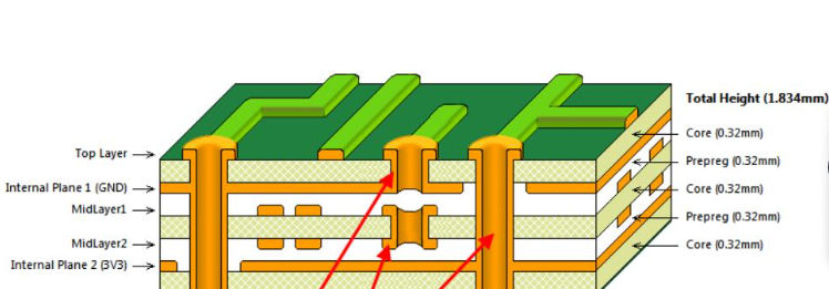
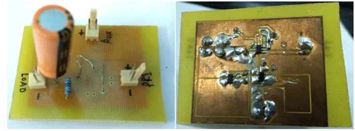
2.5 PCB layout and routing issues
PCB layout and routing also have an important impact on the oscillation performance of the DCDC boost circuit. Unreasonable layout and routing may cause parasitic inductance and parasitic capacitance to increase, thereby forming an LC oscillation circuit. This oscillation not only affects the stability of the output voltage, but also may damage circuit components. In addition, impedance mismatch of PCB traces may also cause signal reflection and interference, further affecting the oscillation performance of the circuit.
2.6 Load changes
Load changes may also affect the oscillation performance of the DCDC boost circuit. When the load suddenly increases, the circuit needs to provide more current to maintain the output voltage stable. If the switch tube cannot respond in time or the inductor cannot provide sufficient energy support at this time, the output voltage will drop or even the circuit will not be able to maintain oscillation.
3.Solution strategy
3.1 Increase input voltage
Ensure that the input voltage is within the range allowed by the circuit, and adjust the input voltage as needed to meet the working requirements of the circuit. If the input voltage is too low, consider adding additional power or using a boost pre-regulation circuit to increase the input voltage.
3.2 Check and replace the switch tube
Regularly check the performance status of the switch tube to ensure that it is working properly. If the switch tube is found to be damaged or poorly performing, it should be replaced with a switch tube of the same model or better performance in time. At the same time, pay attention to selecting the appropriate switch tube model and specification to meet the circuit requirements.
3.3 Optimize inductor selection
Select a suitable inductor according to circuit requirements and load characteristics. Pay attention to the selection of parameters such as inductance value, internal resistance and saturation current to meet the stability and efficiency requirements of the circuit. At the same time, consider using high-quality inductors to reduce parasitic parameters and losses.
3.4 Optimize drive circuit design
Design a reasonable drive circuit to ensure that the switch tube is provided with sufficient drive capability and a stable drive signal waveform. Use appropriate drive chips and circuit design methods to improve the performance and reliability of the drive circuit. At the same time, pay attention to the matching problem between the drive signal and the switch tube to avoid signal reflection and interference.
3.5 Optimize PCB layout and routing
Use reasonable PCB layout and routing strategies to reduce parasitic inductance, parasitic capacitance and impedance mismatch. Pay attention to maintaining the integrity and continuity of the signal line to reduce signal reflection and interference. At the same time, use appropriate grounding strategies and shielding measures to improve the anti-interference ability and stability of the circuit.
3.6 Increase load adaptability
Design a DCDC boost circuit with load adaptability to cope with the impact of load changes. For example, use the method of dynamically adjusting the switching frequency and duty cycle to keep the output voltage stable; or use soft start technology to reduce the current impact during the startup process.
4.Conclusion
The failure of the DCDC boost circuit to oscillate is a complex problem involving multiple factors. By deeply analyzing the causes and taking effective solutions, we can effectively solve this problem and ensure the normal operation of the circuit. In future designs and applications, we need to pay more attention to the details of the circuit and performance optimization to improve the reliability and stability of the circuit. At the same time, with the continuous advancement of technology and the continuous expansion of application scenarios, the DCDC boost circuit will play an important role in more fields.