Are you still using the method of splicing capacitors to suppress EMI?
With the development of technology and the advancement of science and technology, electronic and electrical products are moving towards smaller size and lighter weight, and are also entering more markets, such as automation, automobiles, instrumentation, and medical.
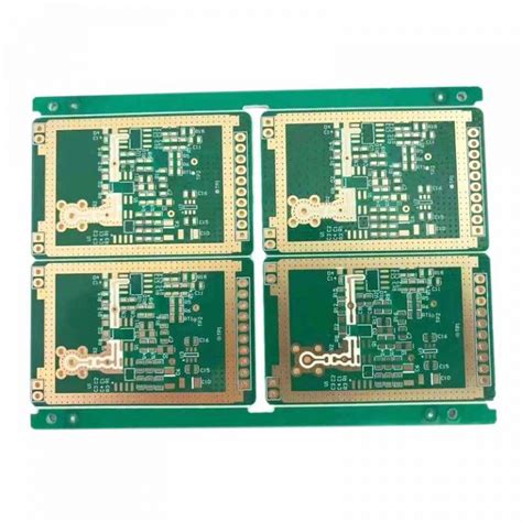
Electronic devices are facing challenges such as increasingly powerful functions and increasingly smaller PCB sizes.
In order to achieve the best design, system designers need to repeatedly weigh performance and functions, which may affect the design and mass production of products. How to add the required functions in a very limited space and meet regulatory requirements (such as electromagnetic interference standards) requires more integration at the integrated circuit level to achieve more intelligent packaging.
Electromagnetic interference (EMI) testing is a test that must be done before a product is launched on the market, because in a complex electromagnetic environment, any electronic and electrical product should not only be able to withstand certain external electromagnetic interference and maintain normal operation, but also should not produce unbearable electromagnetic interference to other electronic and electrical equipment. Therefore, more and more products must pass EMI standards before manufacturers can obtain commercial sales qualification certification for products.
However, it is reported that more than 50% of product designs cannot pass EMI testing at one time, so products must fully consider EMI issues at the design stage.
Therefore, an important step in isolation-based circuit design is to supply power and transmit data across the isolation barrier. Conventional DC-DC converters may be effective, but there are usually trade-offs. These methods may include using discrete circuits and transformers to transmit power. Transformers are usually bulky, require many external components, and take up valuable PCB space, which is not applicable in an era where electronic components are required to be smaller and smaller.
Now, a more efficient and cost-effective solution is to integrate transformers on the circuit and use smaller chip-scale packages. About 10 years ago, Analog Devices invented isoPower, which can transmit power across the isolation barrier using a small solution. The functional block diagram of this device is shown in the figure below. The chip package also integrates 4 isolation channels for high-speed data transmission. This is an optimized solution that does not require the design of power supply. While reducing the size, it also includes EISA isolated DC-DC converters and provides chip-scale packaging, which greatly improves the power supply capability of limited systems.

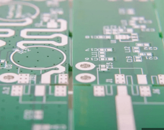
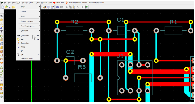
Overlap stitching capacitors are used for multi-layer PCBs, 2 layers of power plus 2 layers of signal
The more devices integrated on the circuit, the more radiated emissions. A common method of reducing radiated emissions at the PCB level is to reduce the level of radiated emissions by forming a low impedance path from the secondary to the primary through the common-mode current.
This can be achieved by using stitching capacitors between the primary and secondary sides, but discrete capacitors are expensive, bulky, and take up valuable PCB area, especially where multiple components may be stacked at the isolation barrier, and this method usually only works at lower frequencies.
Another solution is embedded stitching capacitors, which usually require 4 layers of PCB. The parallel capacitance formed by such capacitors has extremely low inductance and is effective over a very large frequency range (over 1 G), but since the PCB requires 4 or more layers, it greatly increases the complexity and cost of the design. Therefore, using stitching capacitors instead of discrete capacitors or embedded capacitors does not effectively solve the problem of radiated emissions.
The ideal solution is to not use stitching capacitors, reduce costs and PCB design complexity, which requires a component-level solution that does not require the use of complex and expensive external components to avoid high radiation. ADI’s new generation of isoPower solutions ADuM6421A that supports isolated data uses innovative technology to avoid large amounts of radiation on two layers even without using stitching capacitors. To reduce radiated emissions, the device has excellent coil symmetry and coil drive circuits, which can significantly reduce the common-mode current transmission across the isolation barrier, thereby reducing the factors that cause radiation, especially by reducing the noise density at a specific frequency through spectrum technology, so that the radiation energy can be dispersed over a wider frequency band.
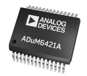
The ADuM6421A integrates a DC-DC power converter with data isolation. It is small in size and has excellent radiated emission performance. It is a cost-effective and low-complexity solution that helps to meet radiated emission regulations. For a 2-layer PCB board, its isolation power is 500 mW, and even under this load, it can meet CISPR 32 Class B requirements with a large margin. This product uses a 28-pin fine-pitch package with a minimum creepage distance of 8.3 mm. Note that its footprint is the same as that of a 16-pin wide-body SOIC package. Therefore, even if this package has a small pitch, the space occupied is still the same. In addition, the ADuM6421 has four high-speed data channels and has good electrical noise and electromagnetic interference suppression capabilities.
The figure below shows the board area and cost savings that can be achieved by using the ADuM6421A. As mentioned earlier, chip-level or even discrete DC-DC converters often require stitching capacitors to achieve CISPR 32 Class B requirements; embedded stitching capacitors typically provide better performance than discrete capacitors, but the PCB must have at least four layers. The ADuM6421A can solve all of these problems. It supports two-layer PCBs and can achieve CISPR 32 requirements under 500 mW load conditions. Compared with a four-layer solution, the use of the ADuM6421A can save up to 70% of the PCB area, and use a two-layer PCB to save 30% of the cost.

ADuM6421A Advantages: Simple, Small Size 2-Layer PCB
Summary
EMI in power products has always been a challenge. Integrated isolated power supplies using isoPower® chip-scale transformer technology have changed the design of isolated systems. This technology simplifies the process of building and verifying independent isolated power supplies, reduces board size, and can achieve low EMI design without the use of multiple discrete components. In particular, the new generation isoPower solution ADuM6421A with isolated data has the characteristics of low radiation emission, small package size and high operating temperature, which can meet the needs of safety-critical applications, as well as the requirements of stringent leakage current, compact and intensive design. Using this device, the difficulty of certifying new applications for new projects can be reduced without high-cost EMI suppression technology.