Basic Steps for PCB Copying/PCB Design
PCB Design Step 1: Preliminary Work for PCB Copying
- Use a schematic design tool to draw a schematic and generate the corresponding netlist. Of course, in some special cases, such as when the circuit board is relatively simple and a netlist is already available, you can skip the schematic design and directly enter the PCB design system. Within the PCB design system, you can directly access the component footprints and manually generate the netlist.
- Manually Modify the Netlist: Define component mounting pins and other pads not on the schematic to their corresponding nets. Define pads without any physical connection to ground or protective ground, etc. Change the pin names of components whose pins differ between the schematic and the PCB footprint library to match the pin names in the PCB footprint library, especially for diodes and transistors.
PCB Design Step 2: Create a Customized Footprint Library for Non-Standard Components
It is recommended that you place all your drawn components into a dedicated design file for your own PCB library.
PCB Design Step 3: Set up the PCB Design Environment and Draw the PCB Frame, Including the Center Hollow
- After entering the PCB copying system, the first step is to set up the PCB design environment, including the grid size and type, cursor type, layer parameters, routing parameters, and so on. Most parameters can be left with the system defaults. Once set, they will suit your personal preferences and will not need to be modified later.
- Plan the PCB, primarily determining the PCB frame, including the board dimensions. Place appropriately sized solder pads where mounting holes are needed. For 3mm screws, use pads with an outer diameter of 6.5-8mm and an inner diameter of 3.2-3.5mm. For standard boards, these can be imported from other boards or from PCB Designer.
Note: Before drawing the PCB ground frame, be sure to set the current layer to a Keep Out layer, meaning routing is prohibited.
PCB Design Step 4: After opening all required PCB copy library files, load the netlist file and modify the component footprints.
This step is crucial. The netlist is the heart of PCB automatic routing and the interface between schematic design and printed circuit board design. Only after loading the netlist can circuit board routing begin.
During the schematic design process, ERC checks do not address component footprints. Therefore, component footprints may be forgotten during schematic design. When importing the netlist, you can modify or supplement component footprints based on the design.
Of course, you can also manually generate a netlist and specify component footprints directly within the PCB.
PCB Design Step 5: Arrange the layout of component footprints on the printed circuit board, also known as component layout.
Protel 99 can perform both automatic and manual layout. To use automatic layout, run the “Auto Place” command under “Tools.” This command requires patience. The key to successful routing is layout, and most designers use manual layout. Select a component with the mouse, hold down the left mouse button, and drag it to your desired location. Release the left button to lock it. Protel 99 adds several new layout techniques. New interactive layout options include Auto-Select and Auto-Align. Auto-Select allows you to quickly gather components with similar footprints, then rotate, expand, and organize them into groups before moving them to the desired location on the board. Once a simple layout is complete, use Auto-Align to neatly expand or contract a group of components with similar footprints.
Tip: During Auto-Select, use Shift+X or Y and Ctrl+X or Y to expand and contract the selected components in the X and Y directions.
Note: Component layout should take into account mechanical structure heat dissipation, electromagnetic interference, and future wiring convenience. Arrange components related to mechanical dimensions first and lock them in place. Then, move to larger, space-consuming components and core circuit components, followed by smaller peripheral components.
PCB Copying Step 6: Make appropriate adjustments and then lock all components in place.
If space permits, you can include a wiring area similar to a breadboard. For large boards, add more mounting screw holes in the center. Mounting screw holes should also be added near heavy components or large connectors, which bear loads. If necessary, place test pads in appropriate locations, preferably in the schematic. Enlarge any vias that are too small, and define all the nets for the mounting screw hole pads as ground or protective ground.
After placing them, use the VIEW3D function to inspect the results and save the file.
PCB Design Step 7: Setting PCB Routing Rules
Routing rules define various routing specifications (such as the layer used, line widths for each group, via spacing, and routing topology). These can be exported from other boards in the Design-Rules menu and then imported into this board. This step doesn’t need to be set every time; it can be done once, depending on your preference.
Selecting Design-Rules generally requires resetting the following:
- Clearance (Routing tab, Clearance Constraint)
This specifies the required distance between trace pads, vias, and other components of different nets on the board. For typical boards, this can be set to 0.254mm; for boards with relatively open spaces, 0.3mm; and for boards with denser SMDs, 0.2-0.22mm. A very small number of PCB fabricators have a production capacity of 0.1-0.15mm, but you can set this value with their approval. Values below 0.1mm are strictly prohibited.
- Routing Layers and Direction (Routing tab, Routing Layers)
This section allows you to set the routing layers to use and the primary routing direction for each layer. Please note that single-sided boards for surface-mount boards use only the top layer, while single-sided boards for through-hole boards use only the bottom layer. However, the power plane for multilayer boards is not set here (you can add it in the Design > Layer Stack Manager by clicking the top or bottom layer, then using Add Plane. Double-click to set it, or delete it by clicking the layer). Neither are mechanical layers set here (you can select the desired mechanical layer in Design > Mechanical Layer and choose whether it is visible and whether it should be displayed in single-layer display mode).
Mechanical Layer 1 is generally used for drawing the board border;
Mechanical Layer 3 is generally used for drawing mechanical components such as board rails;
Mechanical Layer 4 is generally used for drawing rulers and annotations. You can see this by exporting a PCAT-structured board from the PCB Wizard.
- Via Shape (Routing Via Style in the Routing tab)
This specifies the inner and outer diameters of vias generated during manual and automatic routing. It is divided into minimum, maximum, and preferred values, with the preferred value being the most important. (The same applies below.) 4. Trace Width (Width Constraint in the Routing tab)
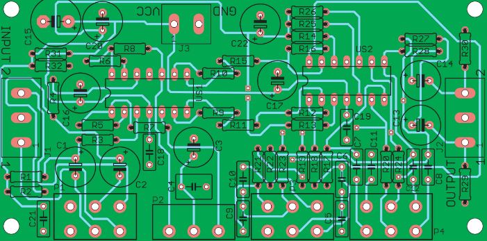
This specifies the width of traces used for both manual and automatic routing. The board-wide preference is generally 0.2-0.6mm. In addition, some net or net class widths are set, such as ground, +5V power, AC input, power output, and power groups. Net groups can be predefined in the Design-Netlist Manager. Ground is typically 1mm wide, while various power lines are typically 0.5-1mm wide. The relationship between trace width and current on a printed board is roughly 1 ampere per millimeter of trace width. For details, please refer to relevant documentation. If the preferred trace diameter is too large for automatic routing of an SMD pad, the trace will automatically be reduced to a width between the minimum width and the pad width at the point of entry. The Board constraint is the width constraint for the entire board and has the lowest priority, meaning that the width constraints of nets and net groups are satisfied first during routing. The following figure shows an example.
- Copper Connection Style Settings (Polygon Connect Style in the Manufacturing tab)
It is recommended to use the Relief Connect method with a Conductor Width of 0.3-0.5mm and four conductors at 45 or 90 degrees.
The rest of the settings can generally be left at their default values, but items like routing topology, power plane spacing, and net length for connection shape matching can be adjusted as needed.
Select Tools > Preferences. In the Options tab, under Interactive Routing, select Push Obstacle mode (when encountering different nets, routes are pushed aside; Ignore Obstacle passes through; Avoid Obstacle blocks). Also select Automatically Remove (automatically removes unnecessary routes). You can also modify the Track and Via settings in the Defaults tab, but generally, they don’t need to be modified.
Place filler layers in areas where you don’t want traces, such as the heat sink and the wiring layer beneath a horizontally placed two-pin crystal. For soldering, place filler layers in the corresponding areas of the top or bottom solder.
Setting wiring rules is also a key aspect of printed circuit board design and requires extensive practical experience.